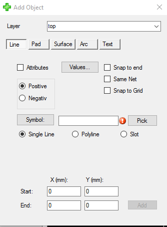
The add dialog can be reached through edit » Add and offers basic editing capabilites one might already know from MS Paint.
Layer: The first dropdown specifies the layer the changes are made on. By default the topmost active layer is selected.
DropDown-Options: The dropdown is followed by five buttons representing the five ODB++ standard object types: line, pad, surface, arc and text. (For more information to dynamic text click here!). Each with their own slightly different "drawing" options depending on their data properties. Clicking the respective button lets you determine, which object type you'd like to add.
The Attribute Checkbox: ODB++ offers a magnitude of different attributes you can add to your PCB layout in a standardized format, optional, but needed for a variety of analyses. For example the design rule check, you need to know, if a drill hole is plated or unplated, since an unplated one needs a greater distance to copper to avoid short curcuiting. The Attribute checkbox determines, if the values you choose through the Value button are actually shown or not.
The Value Button: Offers you the possibility to add values to these ODB++ standard attributes (regardless of the currently selected object type) and append them to your currently selected layer. Adding a value automatically actives the Attribute Checkbox. Please note, that each attribute expects a specific data type ranging from ints and floats to strings.
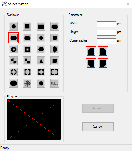
The Symbol Button: Lets you choose, which "pen" you'd like to draw with. The symbols correspond to the in shapes/D-Codes defined in ODB++. If you know the exact designation, you can enter it in the empty input box. Each shape can be further customised in turn in accordance to their attributes, for example, setting a diamter for arcs or specifying, which corners should be squared or rounded, when using a squared "pencil".
The Pick Button: Offers you the opportunity to assume the attributes of an object by clicking on it in the visualisation (as long as it is no surface because surfaces have no attributes). If the attributes have successfully been assumed, the< can be seen by the designation input field. If there is text in it, it worked.
The Snap to end Checkbox: Activating this option allows you to click in the proximity of an object in the visualisation and the alogrithm sets the starting point of your line to the end point of the clicked object.
The Same Net Checkbox: Activating this option allows you to add nets from overlapping elements.
Drawing angles with lines and polylines: Holding the shift key pressed while drawing lines or polylines allows you to switch from a free angle selection to a selection mode that adds exactly 45 degrees with every step you move your mouse.
X/Y Coordinates: Like in many cases in PCB-Investigator, here you have the possibility of adding objects via inserting the exact x and y coordinates, wherever you want your object drawn.
Snap to Grid Checkbox: Activating this option snaps the path of the object you are drawing, especially lines, to the grid model which you can customise via Start » Options » Tab Grid.
Significant changes should be made using the PCB layout program of your choice with a version control option and distinctly more features, where this particular step of the formation process of a printed curcuit board is concerned. PCB-Investigators edit function is primarily intended to make smaller adjustments and quickly visualising suggestions to give to your layouter. Edit allows you to quickly change values of a selected object. One common use case would be optimising your design for the application of soldering paste by editing pads to require less paste.