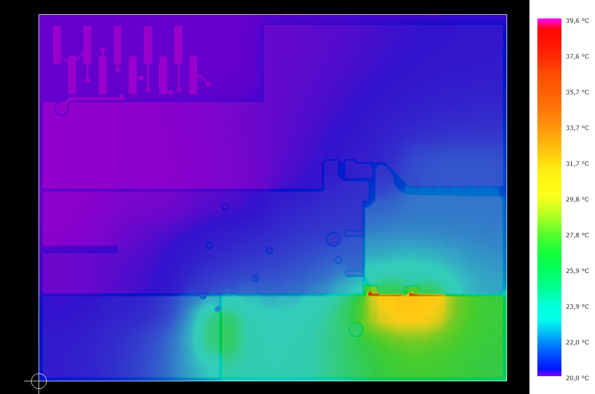
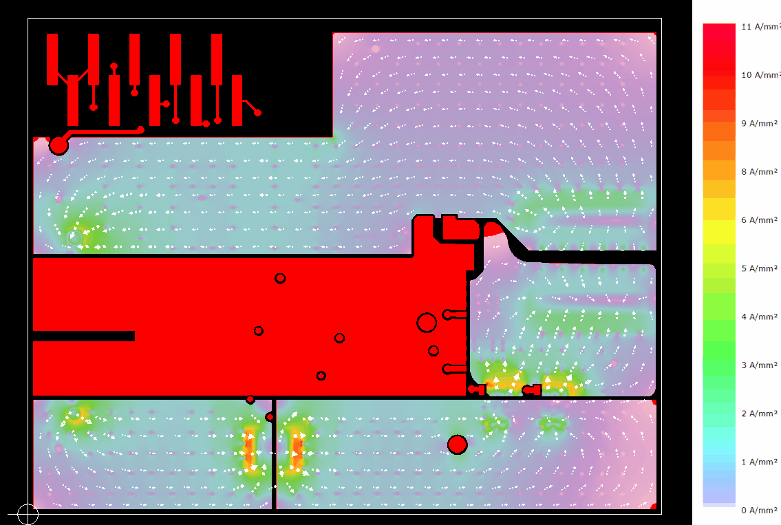
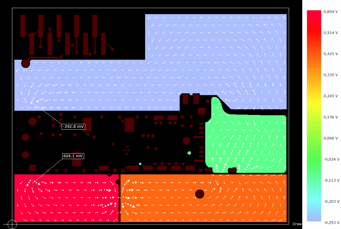
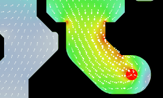
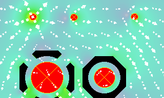
Results: The field solvers calculate values for each simulation point according to raster and layer stack. Base variables are electric potential and temperature. Derived values are current density (vector field), resistance, electric flux and heat flux. The results are accessible by “overlay” plotting on the artwork or in tabular form.
The “Result Viewer” opens automatically when the solution is finished or cancelled.
The last simulation result is automatically loaded, but it is also possible to load former results or import/export results from/to any location
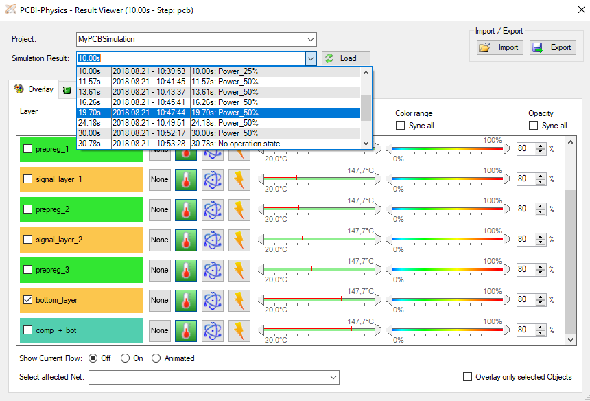
You get a detailed result for every simulation point you have defined.
Default background display is the artwork. Results are additional “overlay data”.
Layer (1):
Activate the layer or prepreg for which you want to see the results. When activating one layer, all other layers are deactivated to keep the clearness. If you really want to display more then one layer including its overlay at the same time, please activate the layers in the normal layer list of PCB-Investigator.
Overlay data (2):
Temperature (°C)
Current density (A/mm²)
Voltage Drop (V)
Value range (3):
By default the overall minimum/maximum values are set. Small red markers show the minimum/maximum values on this layer. You can set minimum and maximum value you want to see in the overlay, e.g. only everything which is hotter than 50°C.
Color range (4):
The range of colors ,which should be used for the selected value range. You can also right click on this slider and then define any value range you want to have.
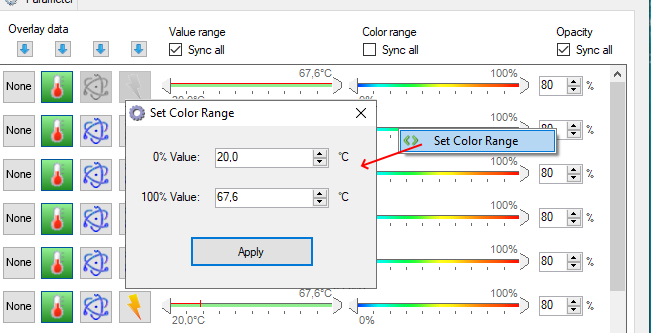
This makes especially sense when comparing two results, e.g.:
By default, red is at 90°C in the first result, and red is at 110°C in second result. But when you define a fix value range from 20°C to 110°C in both cases, colors become comparable, as e.g. yellow will be 70°C in both cases.
Opacity (5):
Saturation of the overlay plot. When defining 100%, the overlay for voltage drop and current density will not be mapped on copper areas only, but will show the real simulated area. There might be a slight mismatch to the CAD copper artwork due to the used raster.
Show Current Flow/ Animation (6):
Select affected Net (7):
Select a net or use the mouse wheel to scroll through all nets. The opacity is reduced for all other nets.
Overlay only selected Objects (8):
The overlay is only shown above selected elements/nets, in this way a certain net can be better reviewed.