Creating a simple example for PCBI-Physics.
Build a simple line example and make a physical simulation for it.
In some steps we create components, nets and stackup to the simple one line example. Then we can start the simulation.
We create a one line example to make a new simple simulation.
In some steps we create components, nets and stackup to the simple one line example. Then we can start the simulation.
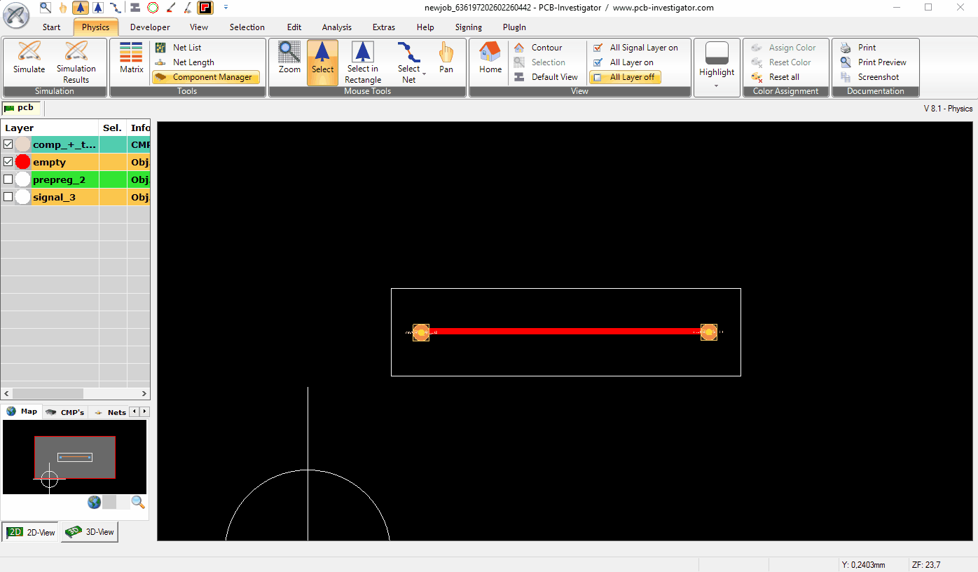
First we need a empty project and add a line. For component connection we use two pads:
Next step is to add components (simulation based on component pins). We use the component editor and create a new package for testpoints from one of the pads. The testpoint package will be added two times: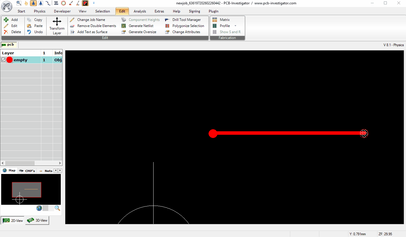
To get clearly defined account defines while simulating, you need to set up a profile. As size is not important in this example , we only need to put a rectangle over all elements (Pay attention: Depending on the accuracy of simulation you need to stick to the mimimum size of the PCB contour):
We build the netlist automatically in the netlist dialog: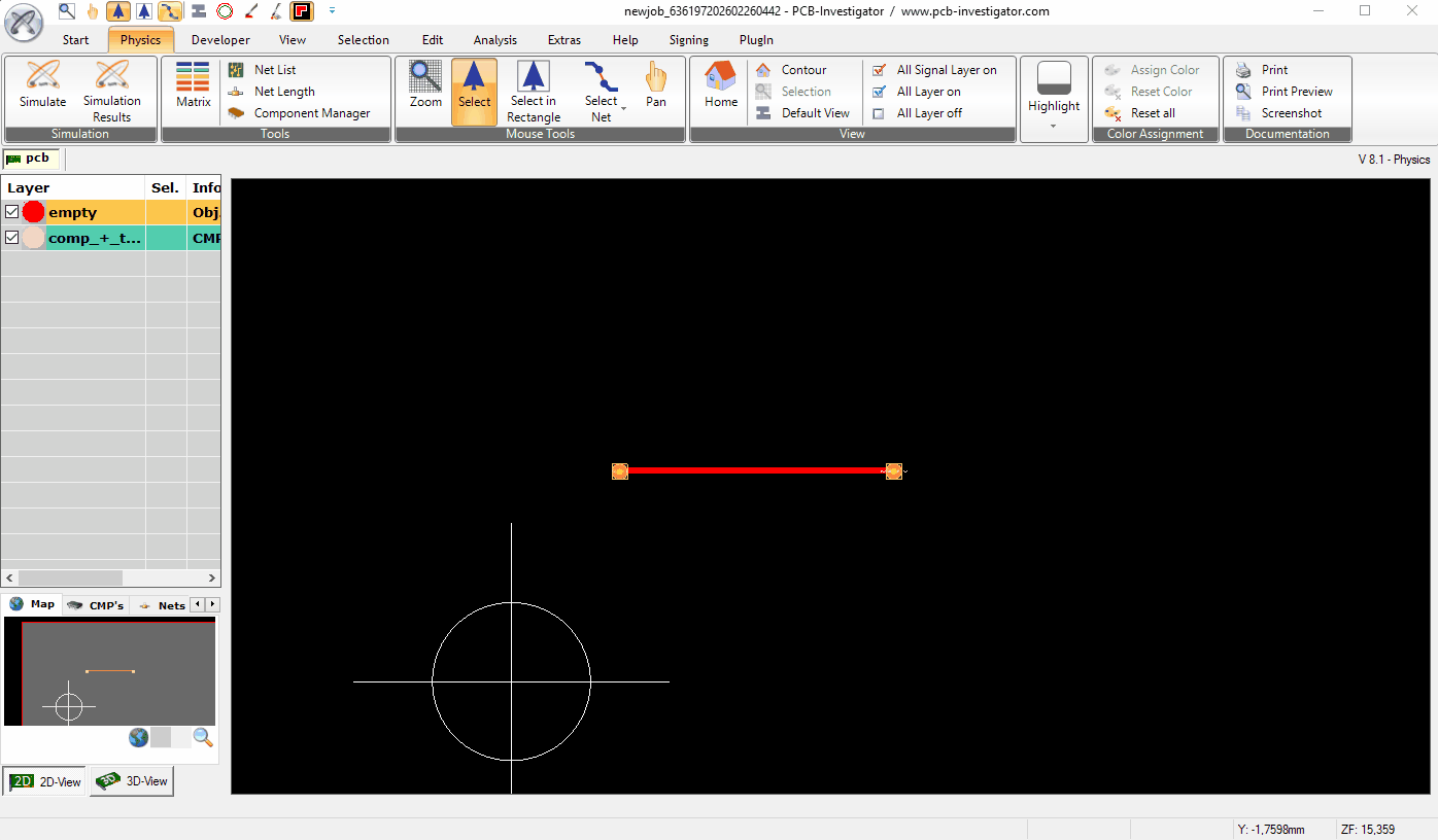
And the layer stackup must contain two signal layer and one dielectric between them. This layers need thickness and correct order. We use the matrix dialog for it: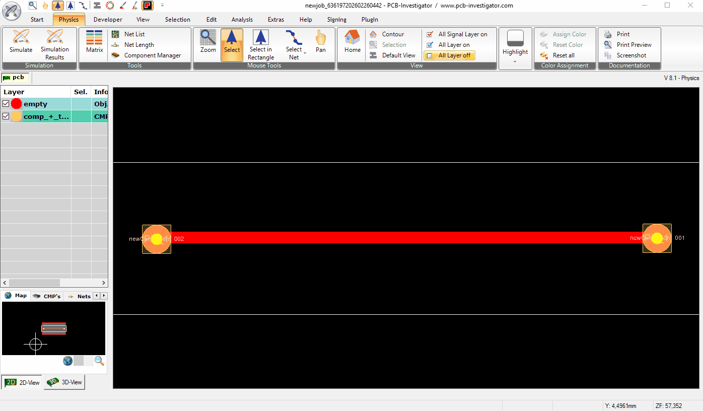
Then we start the simulation: