
 |
Boundary Scan Analysis is used to verify the JTAG infrastructure and determine which component pins can be accessed and tested through Boundary Scan devices and probes. |
Open Boundary Scan Analysis from the PCB-Investigator Analysis area.
The dialog is divided into three main sections. The left side contains the project setup tabs Components, Nets, and Probes. The right side contains Infrastructure Analysis and Interconnections Analysis. The Result Manager in the upper-right area is used to save, load, and delete analysis results.

Use the toolbar to access the main project functions:
When a test program has already been prepared in DFT Preparation, use Import DFT Session before configuring the project manually. The imported session normally provides the component setup, net classifications, and probes required for the analysis. In this case, the corresponding preparation steps can be skipped.
After the import, review the Boundary Scan devices and add the required BSDL files if they are not already assigned. BSDL models are typically not part of the test models created during normal DFT Preparation.
Skip the manual component, net, and probe preparation when a complete DFT session has already been imported. In that case, review the imported data and add any missing BSDL files for the Boundary Scan devices.
When no suitable DFT session is available, open the Components tab before running an analysis.

Assign a suitable model to each component that can be part of a test path. Boundary Scan devices require a BSDL-based model. Other active devices can use digital input, output, or bidirectional models. Passive parts such as resistors, diodes, jumpers, or capacitors should use the corresponding passive model.
To edit a component, select it in the list and open its component information. Depending on the available version and configuration, this can be done by double-clicking the component or by using the edit action next to the properties.
For a Boundary Scan device, import the BSDL information and verify that the JTAG pins are assigned correctly. Typical pins are TCK, TMS, TDI, TDO, and optional TRST. The BSDL model also defines the boundary cells used for input, output, and bidirectional pins.
Use Add Pins as Probe... from the component context menu when selected connector or test-header pins should be used as test access points.
Special exit pins can be configured when the path search should intentionally stop at a specific pin. Use this for transitions to external assemblies or areas that are not part of the current analysis.
Open the Nets tab and review the type of each net.

Set each net to one of the following types:
Signal for normal functional connections.Power for supply nets.Ground for ground nets.The classification is used when pull-up and pull-down paths are evaluated. Incorrect net types can cause paths to be marked as blocking or to be interpreted incorrectly.
Select a net in the list and change its type in the property area. Review supply and ground nets especially carefully before starting the analysis.
Open the Probes tab to check the available test access points.

A probe should be assigned to the correct position, board side, and net. Probes can be imported from a DFT session or created from component pins.
Use the context menu to delete selected probes or clear the probe list. Double-click a probe to locate it in the PCB view and verify that it belongs to the expected net.
At least one probe must be available before the analyses can be started.
Select Settings in the toolbar.

Configure the resistance limits for normal Boundary Scan paths and for pull-up and pull-down connections. Also review the maximum number of hops and the maximum number of infrastructure paths to display.
A path is marked as blocking when it does not satisfy the configured electrical limits or model conditions. When many expected paths are blocking, check the resistance ranges before changing the component or net setup.
A very high hop limit can increase the number of results and the calculation time. Increase it only when valid paths are expected to pass through several intermediate components.
Open the Infrastructure Analysis tab.
Before starting, make sure that the project contains at least one Boundary Scan component, one probe, and one net classified as Signal.
Select Start to calculate the JTAG infrastructure.
The analysis checks the TCK, TMS, and optional TRST connections as well as the TDI/TDO chain between Boundary Scan devices. It also checks pull-up, pull-down, and required compliance conditions where applicable.
The result can be reviewed in the report and graph views.
In the Report View, select a detected chain to display its details. Check whether all expected Boundary Scan devices are listed and whether the chain order is correct.

In the Graph View, use the result list to select the paths that should be shown. Check All displays all listed paths, while Uncheck All hides them.
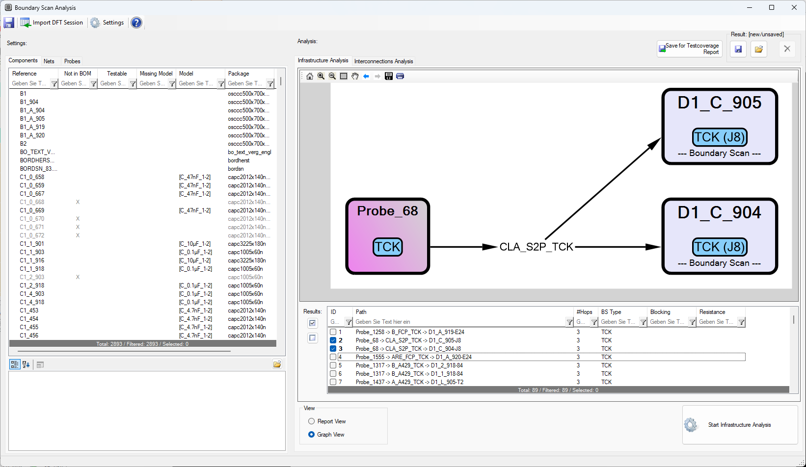
Blocking paths are highlighted in red. When an expected path is missing or blocking, check the BSDL assignment, TDI/TDO mapping, net types, passive models, probes, and resistance limits.
Open the Interconnections Analysis tab.
Select Start to calculate the available test paths between Boundary Scan pins, digital I/O pins, components, and probes.
The result shows which component pins can be driven, observed, or reached through the available Boundary Scan infrastructure and test access points, and which connections are blocked or unavailable.
Use the Report View for an overview of accessible components and pins.

Use the Graph View to inspect an individual path and identify where it stops or becomes blocking.

The default result list shows one row per path. It includes the start and end points, intermediate components, number of hops, path type, resistance, and blocking state.
Enable View Paths per Pin to switch to the pin-based result view. Each pin is then shown with one of the following states:
OK means that at least one usable path exists.Blocking means that paths were found, but none satisfies all requirements.No Path means that no suitable path was found.Select a row to highlight the related path in the graph. Use this view together with the Components, Nets, and Probes tabs to correct the setup.
When a path is marked as Blocking or No Path, check the affected path in the graph first.
Then review the following items:
Run the analysis again after correcting the setup.
Use Save Project to store the component models, net types, probes, and analysis settings in the job.
Use the Result Manager to save the calculated analysis result. A saved result can be loaded again without recalculating the paths.
Use Import DFT Session when a test program has already been created in DFT Preparation. The imported session can provide the component setup, net classifications, and probes, so these preparation steps do not need to be repeated manually. Review the imported data before running the analysis and assign any missing BSDL files to the Boundary Scan devices.
Boundary Scan results can also be used in the PCB-Investigator Test Coverage Report.
For a new project, use one of the following starting points: