Data Preparation

Generally, the services of PCB-Investigator come into play when the layout of a PCB has already been completed. Nevertheless it is possible to make smaller adjustments, where production preperation is concerned. For example, correcting angles that are pointed to such an extent that they can no longer be properly etched.

Adding new Non-Components

Fig 1. - PCB-Investigator Add Dialog
Fig 2. - PCB-Investigator Select Symbol Dialog

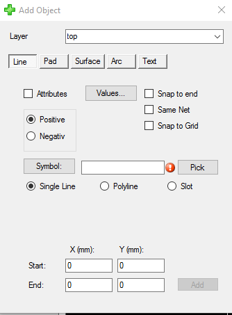
The add dialog can be reached through edit » Add and offers basic editing capabilites one might already know from MS Paint.

  • Layer:
    The first dropdown specifies the layer the changes are made on. By default the topmost active layer is selected.
  • DropDown-Options:
    The dropdown is followed by five buttons representing the five ODB++ standard object types: line, pad, surface, arc and text. (For more information to dynamic text click here!). Each with their own slightly different "drawing" options depending on their data properties. Clicking the respective button lets you determine, which object type you'd like to add. 
  • The Attribute Checkbox:
    ODB++ offers a magnitude of different attributes you can add to your PCB layout in a standardized format, optional, but needed for a variety of analyses. For example the design rule check, you need to know, if a drill hole is plated or unplated, since an unplated one needs a greater distance to copper to avoid short curcuiting.
    The Attribute checkbox determines, if the values you choose through the Value button are actually shown or not.
  • The Value Button:
    Offers you the possibility to add values to these ODB++ standard attributes (regardless of the currently selected object type) and append them to your currently selected layer. Adding a value automatically actives the Attribute Checkbox. Please note, that each attribute expects a specific data type ranging from ints and floats to strings.
  • The Symbol Button:
    Lets you choose, which "pen" you'd like to draw with. The symbols correspond to the in shapes/D-Codes defined in ODB++. If you know the exact designation, you can enter it in the empty input box. Each shape can  be further customised in turn in accordance to their attributes, for example, setting a diamter for arcs or specifying, which corners should be squared or rounded, when using a squared "pencil".
  • The Pick Button:
    Offers you the opportunity to assume the attributes of an object by clicking on it in the visualisation (as long as it is no surface because surfaces have no attributes). If the attributes have successfully been assumed, the< can be seen by the designation input field. If there is text in it, it worked.
  • The Snap to end Checkbox:
    Activating this option allows you to click in the proximity of an object in the visualisation and the alogrithm sets the starting point of your line to the end point of the clicked object.
  • The Same Net Checkbox:
    Activating this option allows you to add nets from overlapping elements.
  • Drawing angles with lines and polylines:
    Holding the shift key pressed while drawing lines or polylines allows you to switch from a free angle selection to a selection mode that adds exactly 45 degrees with every step you move your mouse.
  • X/Y Coordinates:
    Like in many cases in PCB-Investigator, here you have the possibility of adding objects via inserting the exact x and y coordinates, wherever you want your object drawn.
  • Snap to Grid Checkbox:
    Activating this option snaps the path of the object you are drawing, especially lines, to the grid model which you can customise via Start » Options » Tab Grid.


Significant changes should be made using the PCB layout program of your choice with a version control option and distinctly more features, where this particular step of the formation process of a printed curcuit board is concerned. PCB-Investigators edit function is primarily intended to make smaller adjustments and quickly visualising suggestions to give to your layouter. Edit allows you to quickly change values of a selected object. One common use case would be optimising your design for the application of soldering paste by editing pads to require less paste.

Transform Layer


Fig 3. - PCB-Investigator Transform Layer Dialog

The transform layer option allows you to transform whole layers. You can shift, rotate, scale and mirror your selection or even whole layers. The checkboxes at the bottom allow you to further adjust the type of transformation:

  • Transform all active layers:
    This checkbox is activated by default and encertains that your transformations are applied to all layers currently activated in your layer stack up. Deactivating it enlarges the transformation dialog with an additional layer stack up overview you can choose the layers from which you want your transformation applied to.
  • Transform only selected objects:
    Activating this option causes only the objects you selected on their respective layers to be shifted.
  • Auto adjust
    There are cases, especially when using a combination of different data formats like Gerber for your copper layers and Excellon for your drill layers, where you get an unwanted offset between your data sets. The auto adjust option is intended for these cases. You simply have to set a reference point in each layer you want to synchronise by clicking into the visualisation PCB-Investigator will then align your layers using the given points. For the sake of simplicity, it is recommended that you use small concise objects you can easily identify and mark on all needed layers.

Change Attributes

Fig 4. - PCB-Investigator Change Attributes Dialog

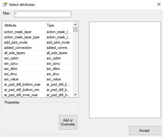
The Change Attributes option can be found via edit » Change Attributes and is very similar in its functionality to the previously described Add option. You get a list of all available attributes and their corresponding types whose values you can change freely via the input box in the bottom left corner. Please note that you have to select an object before the Change Attribute option can be used.

Remove Double Elements

Unclean data sets may contain objects that are basically the same several times lying on top of each other and thus not visible for the naked eye. These double entries would cause errors on many tests and should therefore be removed early on. The Remove Double Elements function which can be fount under edit » Remove Double Elements does just that.

Add Text as Surface

Fig 5. - PCB-Investigator Add Text to Surface Dialog

Add Text to Surface, as the name implies, allows you to add text to your PCB. In this aspect it is similar to edit » Add (Button: Text) the main difference however is that with Add Text to Surface you can change the font while Edit » Add only can use the ODB++ default font. Moreover, edit » Add creates one single text object out of the whole text while in the case of Add Text to Surface every char is an independent polygon (surface). Also, Edit » Add places the text object where you click whereas Add Text to Surface always positions the char surfaces just below the left bottom corner of the PCB.

You can also edit you text dynamically. For more information click here!

Generate Net List

The netlist is an integral part of the inner workings of PCB-Investigator and thus the Generate Netlist function is of utmost importance and is needed especially in two main cases:

  1. Editing the netlist by adding, deleting, dividing, shifting,... destroys the logical links between parts which actually belong together. Generating the netlist anew remedies this by running through all elements of your PCB, identifying which parts are connected and issuing new net names (in case a net name already exists the first net name remains).
  2. File formats like Gerber have no netlists and no net names. Generate Netlist recognizes, which parts are connected and assigns index based names to them and therefore allows you to use all selection methods of PCB-Investigator even those which are based on net names.

Generate Oversize

Fig 6. - PCB-Investigator Generate Oversize Dialog

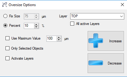
Theoretically, every PCB element can be oversized, but it is arguably most useful utilizing the Oversize function on the soldermask layer. The Oversize function allows you to enlarge each object circumferentially by either a nominal or a percentage value. With especially large objects there also is the possibility to limit the oversize to a fixed µm value. Minimizing is of course also possible. Both variants of the Oversize function, mini- and maximizing, can either be applied to the current selection, each selected, each active, or all layers of the PCB.

A common use case would be ensuring correct margings to counter production-dependent tolerances. If a solder point has the same size defined in your CAD data set as its solder resist recess, it could lead to it being (partially) covered with lacquer in the process of production due to the production-dependent tolerances of 75 µm. Therefore the solder resist mask recesses should circumferentially be larger than the solder pad by 75 µm. If this enlargement wasn\'t already defined in the PCB layout process it can subsequentially be achieved by using the described Oversize function. Furthermore, too small recesses would also be listed as errors while performing a DRC (design role check). PCB-Investigator calls this particular Design Rule Check "Bare Board Check" which is a seperate plugin included in all editions except the Basic one.

Drill Tool Manager

Fig 7. - PCB-Investigator Drill Tool Manager Dialog

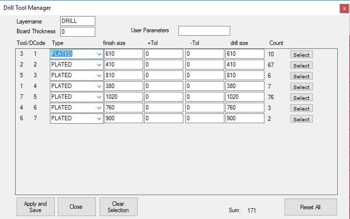
The Drill Tool Manager offers an overview over all drilling tools and information: plated/unplated/via, drilling diameters (the desired diameters the holes should have not the diameters of the drill), number of drill types.

Polygonize Selection

The Polygonize Selection function converts several selected lapping objects to one surface. A common use case would be "pseudo surfaces", which often are used in file formats like Gerber and look like surfaces, but actually are achieved by stringing together several lines. Selecting all these lines and using the Polygonize Selection function, converts them to a true single surface and therefore optimises the data set by reducing file size, increasing the reliability of and accelerating analysis, like e. g. measuring.