 |
A PCB must not get too hot. By using the three-dimensional electric and thermal simulation field solver you predict board, trace and component temperatures under specified heating and cooling conditions. This is reducing the number of prototype trials and saves time in the design phase. |
Components and currents heat up the PCB - but how hot will it get? Will you keep the temperature limits? How long will it take to get too hot? How will a mix of high and low load oscillate?
Neither power dissipation nor electrical current are reliable indicators for the expected temperature. Each printed circuit board is a special case with special losses, layer structure, conductor geometry and cooling environment. Not a single data sheet or internet calculator can tell you how high the expected temperature will be.
PCBI physics is not limited to a maximum number of layers, traces, holes or components. In the first calculation projects, some users will be surprised that their rooted ideas about the flow of electricity and heat won´t be reflected in the results. But you can be sure that the calculation is correct, if the entries and assumptions match. On closer inspection, the result can be explained and understood. Experience has shown that calculation and infrared measurement match very well in a flawless model structure.
What is PCBI Physics?
PCBI physics is more than only a calculator. It is an electrical and thermal 3D field solver.
Allthough current and temperature are based on similar physical descriptions and equations, the technical treatment and the required data are different. For example, voltage calculations require electrical material parameters, sinks and sources in the networks of interest. The electricity is confined to the traces of the board. Thermal calculations require the thermal conducitivity of the material and some information about how the heat is dissipated from the surface to the plate and how it is transported to the surrounding medium. This is the basic effect of surface cooling. But there is also a "volume cooling". The temperature depends on, how layers and prepregs shift the heat within the PCB volume, how thick an seperated they are, how tightly the heating tracks and components are packed and, where the heat can be transported. There are no hard and fast rules for predicting the right temperature. Therefore, a field simulation is indispensable.
Which data do you need?
For the electrical calculation, current or voltage values must be defined for respective networks. As PCB-I knows all PCB details such as number and thickness of layers, trace shape, holes, nets and connections, you are free from any geometric input. All you have to do is to transfer the necessary electrical information from the schematics into a table with networks and pads.
The selection of components and nets for an operating state is very convenient. PCBI physics shows a graph of all involved networks, linked pads and components and automatically fills in current values from the point of current supply to the point of extract. Component losses can also be added here.
As mentioned above, heat must be extracted from the plate. If it is released from the surface into the ambient air, the mechanism will be controlled by the so-called heat transfer coefficient. A built-in wizard calculates this value. If heat is extracted by metallic parts (screws), the temperature of the bolt must be known. You can also assign the thermal resistance of a heat sink.
How fast is PCBI physics?
Field calculations are more complex than spreadsheets and require much more resources because the language of the field is partial differential equations. The results are not available in a flash and solving a 3D field takes computer time. For faster processing, physics is therefore not only developed for CPUs, but also for GPUs. With a good graphics card, the speed gain can be enormous. The results of free convection (also called "still air") on the laboratory bench can best be compared with high accuracy.
This is the first tab of the simulation parameter dialog.
All simulation settings can be imported or exported from/to a xml file by using the “Import Setting” or “Export Setting”(1) button.
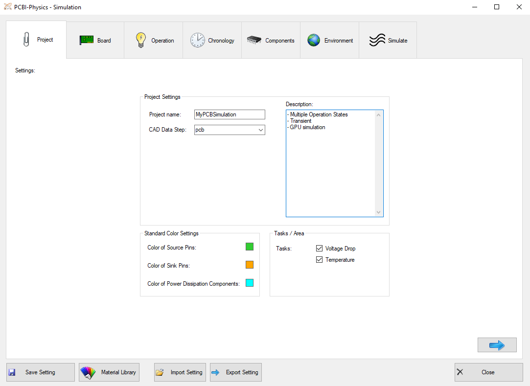
Project Settings (2):
Choose your own project name and descriptive text. They will appear in the result summary file and help to sort your calculation runs.
Standard Color Settings (3):
Pins with current sources or sinks as well as components with power dissipation will be drawn with a predefined color for better recognition. By clicking on the colored rectangles the color can be changed.
Tasks/Area (4):
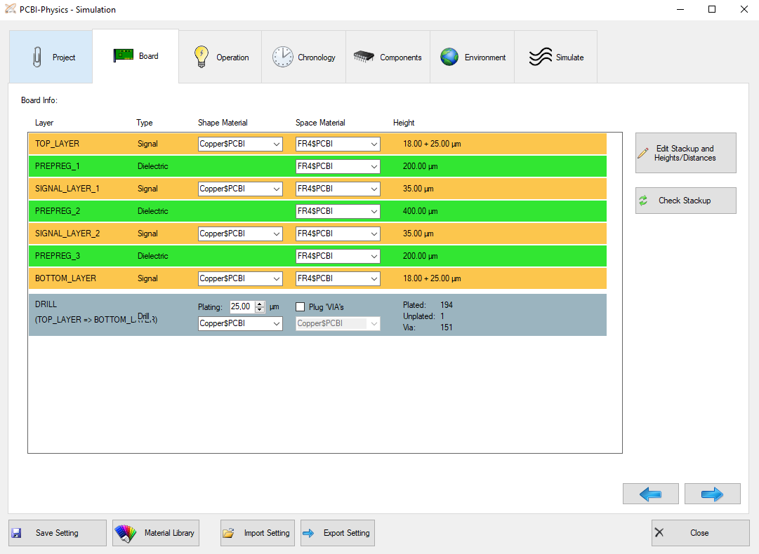
In the ‘Board’ Tab you can check and define the different materials per layer and the general layer stack-up parameters, especially layer heights.
Shape Material:
If the according layer has any CAD elements, the material for those elements can be selected here. Only electrically conductive materials are selectable from the list. For signal layers, “Copper PCBI” is typically the right material. Prepreg layers normally have no CAD elements (Pads, Arefills, Lines, …) on the layer, that’s why this field is hidden. In special cases, also Prepreg layers can contain e.g. a large pad element, which can represent e.g. an embedded copper coin inlay. If such a pad exists, the material for this copper coin inlay can be defined with this field. New materials must be defined in the “Material library” before they can be selected.
Space Material:
The material of empty space on each layer (=area where no CAD elements are) can be defined with this field. Only materials, which are not electrically conductive, are selectable. Typically this is “FR4PCBI”, but also some HighTG Material or even ceramics, glue or other isolation material can be used. New materials must be defined in the “Material library” before they can be selected.
Plating:
The thickness and the electrically conductive material of the plated drill sleeves can be defined for each drill layer. Typically this is 25µm copper. In the simulation model the plating value reduces the end diameter of the hole, so a CAD hole with 300µm and 25µm plating results in a 250µm hole. In ODB++, drill pads can have a property “.drill” with the values “plated”, “non-plated” or “via”. By checking the box “Plug ‘VIA’s”, you can define that all “via” drills are completely filled with the selected electrically conductive material instead of using a conductive sleeve.
Edit Stackup and Heights/Distances:
The layer matrix is opened with this button to add additional layers, change layer heights or reorder the stack-up.
Conditions for a correct stack-up definition:
Important: All other information like “via filling” or material definitions are not used in the simulation and must not be set here!
In the Operation tab, you can define different operation states you want to consider in your simulation.
To do this, you have two different options:
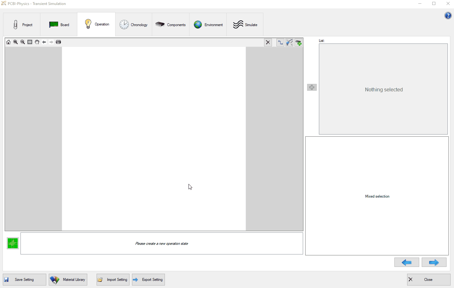
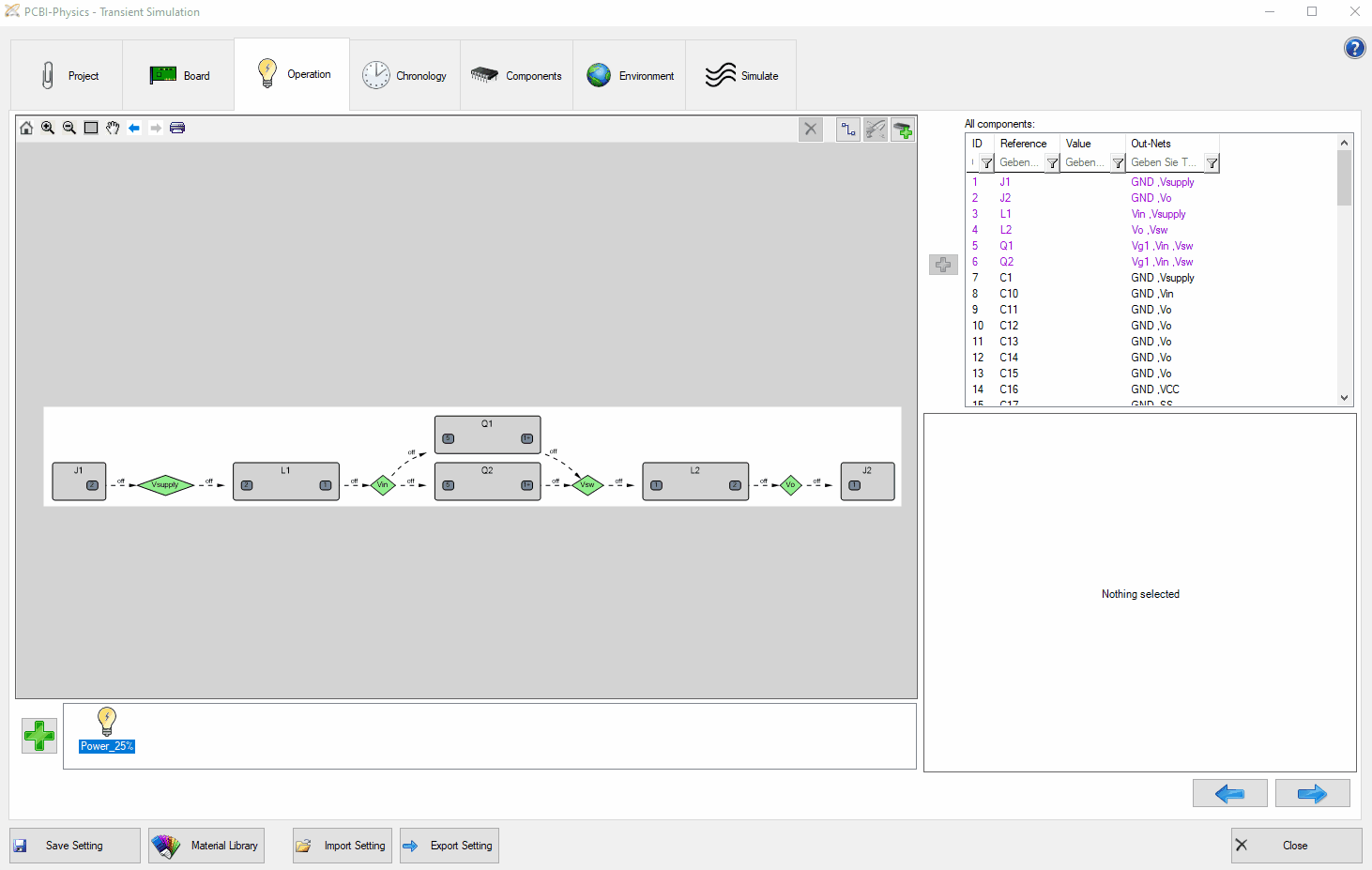
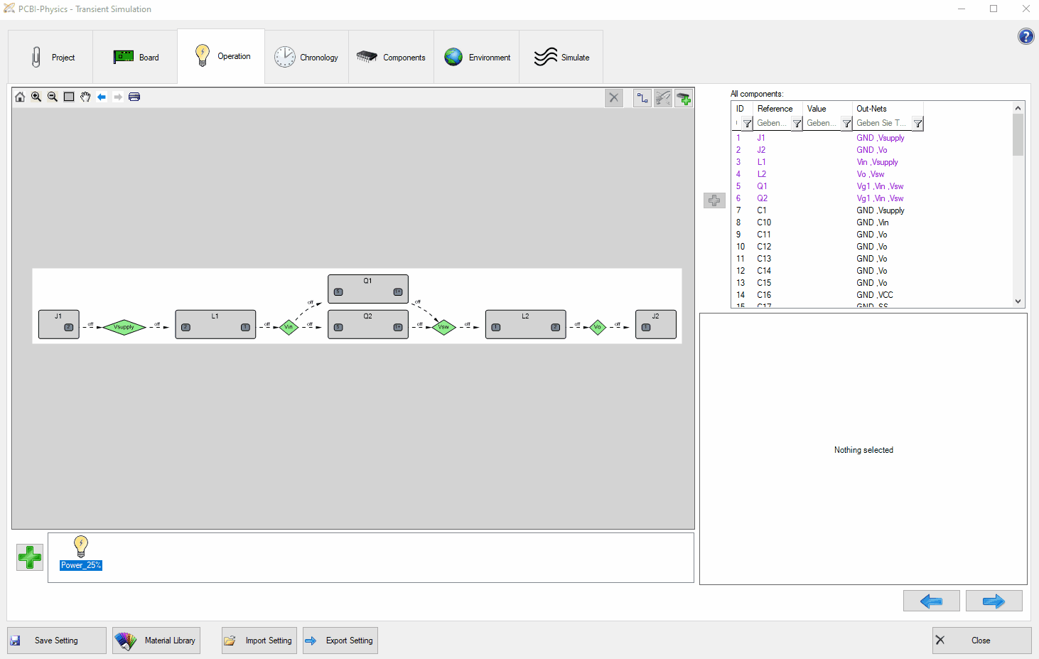
At first you have to create a new operation state by entering an appropriate operation state name. Then, you add the first component from the list which marks the starting point for defining a new operation state. Coming from this component, you choose an available net for the respective component for adding more components that you want to include in the simulation.
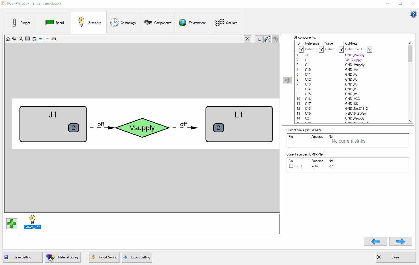
After that first step, you synchronize the selected component in PCB Investigator and add further component pins from the graphic interface as a sink to the net (right click). These two sinks build the basis for the list-based completion of the current path by multi-selecting the two parallel components and thereupon selecting the remaining components to be used for the respective current path.
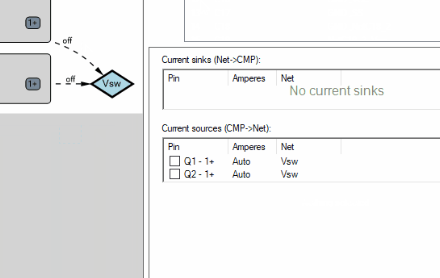
Additional information for the components Q1/Q2: Pin ‘1+’ indicates, that all pins of this component connected to the same net are combined and considered as a single pin for the simulation (e.g. related to the current input). Number 1 in ‘1+’ refers to the name of the first pin in this net.
(Other example: if pin 17 and pin 18 of a component are connected to the same net, the pin name in Physics would be ‘17+’)
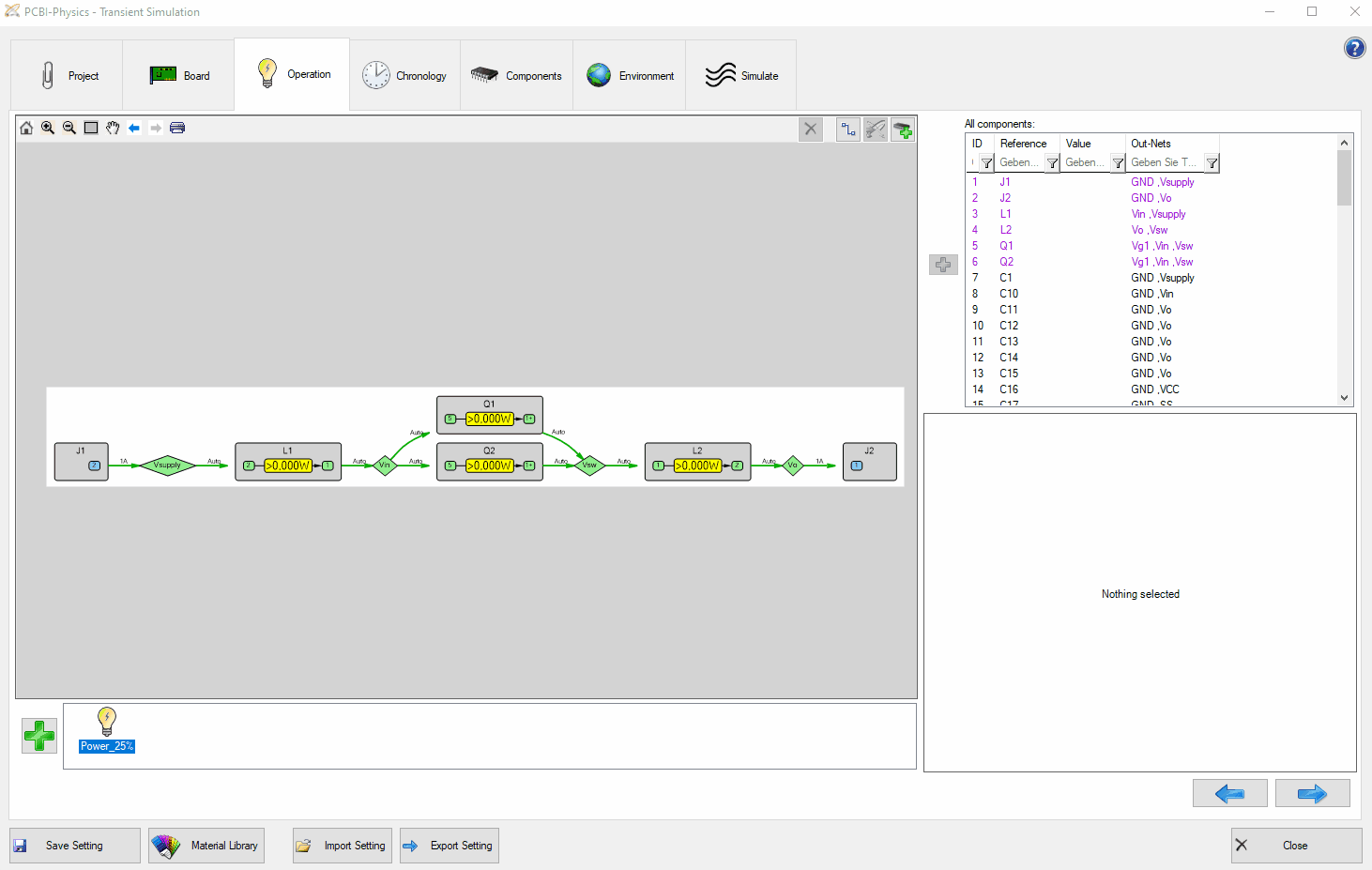
You now have two different options when defining the current flows. On the one hand, you can enter the power losses for each component and currents for each net using the conventional path (1).
On the other hand, there is a new, alternative way via the definition of pin bridges (2). Here, you just define the amount of current which is going through the current path in total, but you do not have to know and enter how the current is split up in each single net of e.g. parallel parts. Furthermore, the input of the power dissipation is omitted as it will be derived during the simulation by using the internal resistance (e.g. RDSON). Especially for parallel components, this input method has advantages, because you do not have to know how the current splits up, as this will be simulated by the tool using net lengths, copper structures, temperature depending material properties and component resistances.
 (1) Now the currents are to be defined. Energize particular nets by directly entering the corresponding values in the graph. Using multiselect, several components are marked and a fixed current can be set / split. The left side of the component marks the sink of the net, the right side the source. Thereby, you always have to keep the sum of the sources and sinks per net identical. It is possible that there are several pins of a component that cling together to only one net. You just have to enter the ampere of each pin. The current arrows then show you the sum. Furthermore, a fixed value for the power dissipation must be determined for each component. This value can be taken from your data sheets.
(2) The energization process can also be realized by defining pin bridges. In this example, the pin bridges are defined for each of the four components, whereby a fixed internal resistance is to be determined. Alternatively, you can specify the internal resistance as temperature-dependent. As soon as you have defined a pin bridge for a component, you can see how the pins within the component are connected graphically by an arrow.
Different from (1) the activation respectively the calculation of the power dissipation is done during the simulation based on the internal resistance of the pin bridges. Therefore, no fixed portion is given, but the formula P = R*I² (power dissipation = resistance x current²) will be applied. In addition, you can determine a fixed proportion as a base. Since the actual power dissipation of a component depends on the current according to the formula mentioned before, you will only find ">0" or ">fixed portion" at this point.
The activation of the current as well as the calculation of the current intensity for sources and sinks is done automatically (see green marking + "Auto"). By defining the pin bridges, the current path between the components is considered as if they were connected to a single large network. The current flows across all components with their defined pin bridges according to the conduction and component resistance. In the case of parallel components, the amperes are divided; the exact distribution results from the simulation, yet, if the internal resistances are the same, a 50:50 distribution can be assumed. Only for the last component in a current path the current has to be defined, in this case 1 ampere.
Copy the given operation state and multiply the currents and power losses with the chosen factor. Then, activate a new path in the operation state that has been inactive before.
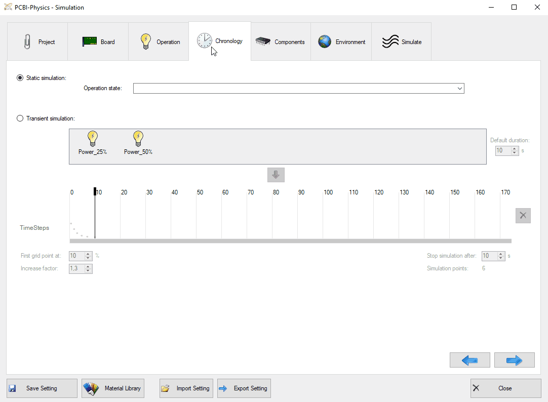
The determination of chronology allows you to perform transient simulations with different simulation states as well as static simulations.
If you opt for transient simulation, you can choose between the different operation states you have previously defined. First, you can define the default duration of the respective operation states. This setting can be adapted by hand even more precisely later. Choosing one of the operation states, you can display it on the timeline. In order to simulate a cooling, the duration of the simulation without an active simulation state can also be adjusted. Further parameter settings would be the definition of the grid/simulation points and the increase factor of the simulation points. At the end, you get a result for each simulation point. The more points you have, the more accurate the result will be but the simulation will also take much more time (the number of simulation points is displayed below). The time duration can also be adjusted with "stop simulation after".
After defining an operation state, you can now add all further passive components into the simulation model.
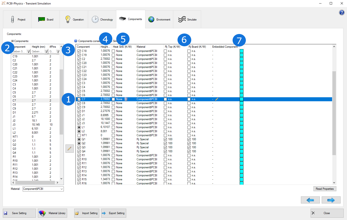
All components considered in the operation states are already included in the table and marked with a painted box (1). You can´t deactivate them as they are powered in the simulation state, but you can add a heat sink and adjust the material.
The list includes all components that will be considered in the simulation.
Therefore: Add all components which will influence the temperature of the board. This includes all components with a defined power loss (heat source) as well as components without power loss, as their existance (defined by size, height and material) also influences the temperature. They do not actively heat, but increase the board surface and by this is contributing to cooling. If you remove components, the result will be more incorrect as it won´t be considered in the simulation.
IMPORTANT: The bodies of components are not allowed to overlap or intersect each other! So please be careful with variants or large shielding components.
Now, select a reference designator (2) and add the components to the list (3). The component material normally is a non-conductive mixture material of plastic an metal. In the global material library, we have predefined three different component materials, low, high and very high metal percentage. For components with a bottom heat slug, we recommend "very high". Of course, you can define own materials, e.g. to simulate a printed component or a glued cermic part.
For all components considered in the simulation, the component height (4) must be defined correctly. The height can be changed/defined by clicking into the height cell of a component entry in the list on the right side. By unchecking a component entry in the list on the right side, you can deactivate this component in the simulation without deleting it from the list.
Another (optional) parameter considered in the simulation is the heat sink (5). The default heat transfer on the surface is replaced by the given thermal resistance (K/W) of an attached heat sink R_HS. Heat sink data must be found in the manufacturer's data sheet. However, a thermal resistance value Rth depends on area A. Only Rth*A is independent of the area. Normally, the data sheet heat sink does not exactly have the same base area as the component. Then, the data sheet value must be converted according to the following rule "Rth_comp = (A_DS : A_comp) x Rths_DS".
(Convert correctly if the data sheet specifications are in inch².)
The two-resistor model (for junction temperature Tj) (6) is a parameter that can also be considered optionally. If you do not specify the value, it is given as unspecified (n.s.). To estimate the junction temperature, you need instructions on how to transport heat from the junction to the surface and/or to the board inside the component. Sometimes you can find these instructions in the component's data sheet. In the model of the component´s body, it is no longer a bulk average but equal to "junction". An isothermal node is created with the help of a material Rj Special. The node is connected to the surface by Rj Top and to the board by Rj Board. The displayed result (numeric and graphical) now is the junction temperature Tj!
Advise:
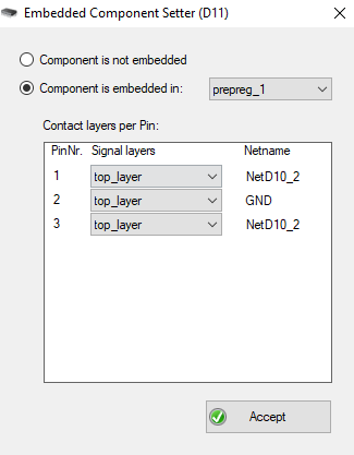
The last optional parameter is Embedded (7) and refers to components that are neither on the top nor on the bottom layer, but on a prepeg layer. The ODB++ format cannot represent this special position of components, but for thermal simulation the exact position of components is quite relevant respectively unnecessary result distortions could occur. Therefore, you can specify - if necessary - whether a component is embedded in a prepeg layer. The corresponding contact layer can also defined at this point.
To achieve a thermal equilibrium, the board has to be cooled. A good cooling environment (e.g. when strong fans are present) will lead to a low temperature and suppressed cooling (e.g. in an enclosure) to a high temperature (at same power).
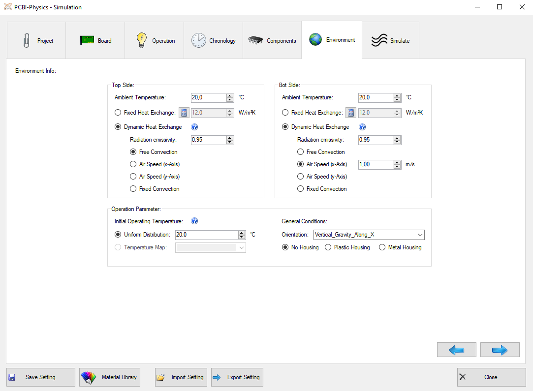
Ambient temperature:
The air temperature in vicinity of top and bottom side.
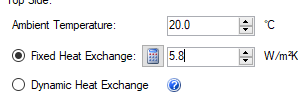
Fixed Heat exchange:
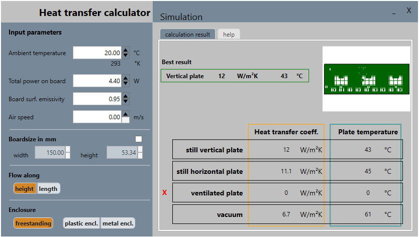
One way to simulate cooling is to perform a hydrodynamic flow field calculation, which is by far too time consuming and not appropriate for our purpose. PCB-I uses an approach known from mechanical engineering. The quantity, which can parameterize the heat flux to the ambient, is called heat transfer coefficient h (W/(m²K)). The larger h, the more effective heat can flow to the ambient. h is not a material property! PCBI-Physics uses a total value h, which is the sum of convective and radiative contribution.
Heat exchange calculator:
A standard value for h is between 10 to 12 W/m2K. But h depends on power, the board size, the board orientation and the ambient air temperature. The calculator gives a good estimate working in most situations.
Dynamic Heat Exchange:
The (total) Heat Exchange is assumed as a sum of a convective and radiative part. This option is available only in transient or pseudo-transient mode, for top and for bootm side.
First, you have to specify the radiation emissivity. Radiation is always calculated at all surface points depending on their temperature and the housing options. Radiation emissivity describes how a material or a body surface exchanges infrared radiation with its surroundings. The maximum emissivity value is 1.
The most commonly used are listed here:
For the convectional part, there are the following three options:
Operating Parameter:
Defining the initial operating temperature, you can choose between a uniform distribution of temperature or the temperature map. Furthermore, you have to determine the general conditions of the board, e.g. if there is a housing (plastic or metal) or not. The orientation is important for the simulation as it affects the convection of the board.
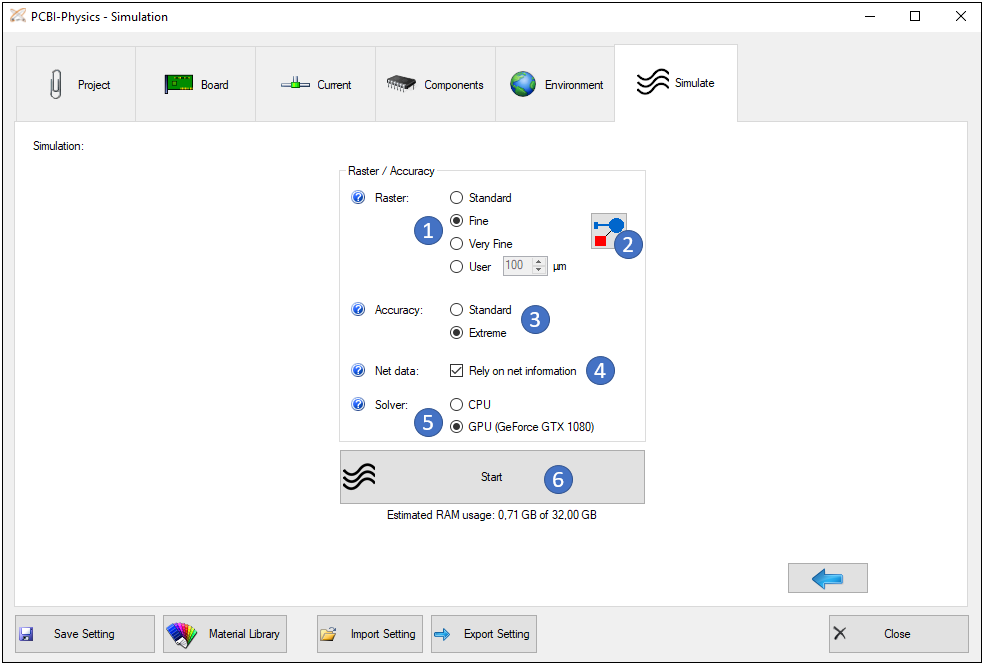
Raster (1):
The solution requires a large set of nodes inside the PCB volume. Define the spacing in x-y-directions. Standard means a spacing of 0.2 mm, fine 0.1 mm and very fine 0.075 mm.
Especially current-carrying traces (only those) need to have at least one, better two, nodes across width. For example the thinnest trace of interest is 0.2 mm wide, then choose at least a raster of 0.15 mm. better take 0.1 mm: The finer the raster, the more computational work. The vertical spacing is defined by the layer stack-up.
The button (2) helps to determine the right raster size by checking all distances between current carrying nets and their minimum trace widths. If nets are too close together or too thin for the chosen raster, this is reported.
Accuracy (3):
The solution of the fields is done with iterative algorithms, starting from zero and ending at a “converged” final state. The decision when to terminate the iterations is controlled by this flag. Standard is stopping the iterations at a relative residual of 0.1%, extreme stops at 0.01%.
Only experience can tell what to take best. Boards having a small number of nodes (either small by geometry or by coarse raster) could need extreme, because they tend to stop too early. Huge number of nodes could be done with standard. In fact, there is a case specific intimate relation between numerical work and how easy physics boundary conditions and geometry allow for an equilibrium.
Net data (4):
It is recommended to check rely on net information.
The electric solver is setting nodes only into the nets with Ampere values. This saves resources and allows a secure treatment.
Solver (5):
In most cases calculations run much faster on graphic cards (GPU) than they do on the universal processor (CPU) (from our experience up to 10x faster). But that depends strongly on hardware properties. GPU is only available for recent Nvidia graphic cards with at least CUDA 5.x support. The graphic card should also have at least 2 GB of RAM, better would be 4 or 8 GB.
Start (6):
Launches the simulations.
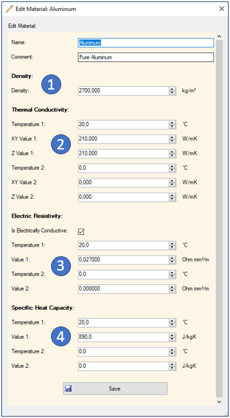
The required material data concern thermal and electric resistivity for steady-state calculations plus specific heat capacity and mass density for time-dependent calculations.
Except density, the properties can be set temperature dependent, but is not demanded. If values are given for “Temperature 1” only, the values are temperature independent. If values are given for two different temperatures, they define an infinite straight line. The “supposed operating temperature” action will take use of it.
Because of the contributions of woven glass and epoxy resin to board base material, the “FR4” thermal conductivity is said to be “orthotropic”. x-,y- and z-directions can have different values. EMV requirements may need denser or lesser dense woven glass and by this influence the conductivity. Ask your provider about experimental values. For “isotropic” materials just type the value twice.
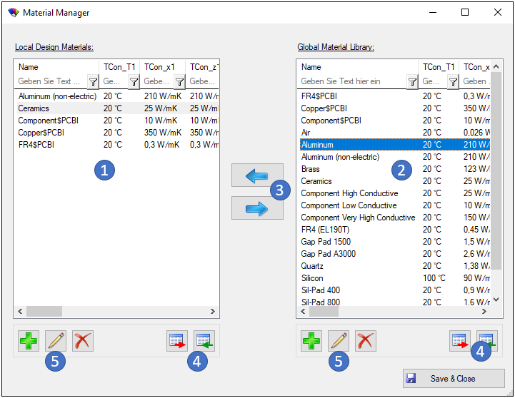
Local design Materials (1): The subset of materials used or available in this board calculation. These material properties are also stored in the project depending simulation setting xml file and can be therefore exchanged with other team members without influencing the global library.
Global Design Materials (2): This is the list of available materials in the global, design independent library.
By using the arrow buttons (3) in the middle of the dialog, materials can be copied between the two libraries.
With the import/export buttons (4) you can export selected materials into a xml file and import it again (on another computer for example).
With the buttons “Add”, “Edit” or “Delete” (5) you can create new materials, edit the material properties or remove a material from the lists. Materials ending with “PCBI” can not be changed or removed.
Density (1): This parameter is not used yet in the simulation, as the temperature variations of density can be ignored.
Thermal conductivity (2): Enter data at least for 1 temperature point.
Electric resistivity (3): If the material is an insulator (dielectric), don´t to anything. Else check and give a value at least for Temperature 1. Note the physical unit. You can also uncheck “Electrically Conductive”, e.g. aluminum to simulate the right thermal behavior without having to take care about possible short circuits when using Aluminum layers or inlays.
Specific Heat Capacity (4): Give a value at least for Temperature 1. Note the physical unit. (These parameters are not used yet in the simulation).
While iterations are running, the convergence is displayed. The blue line is so-called residuum. The iterations are terminated, when the value has dropped to about 0.1% of the initial value or 0.01%, resp..
The thermal simulation:
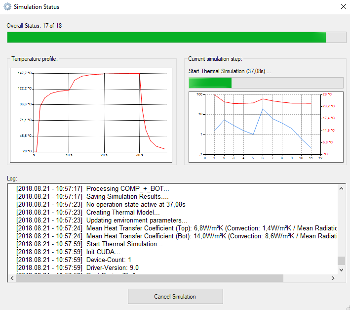
The thermal calculation has an additional red line for the maximum temperature. In this example, you can see the rise of the temperature during during the two simulation states and the simulated cooling as the red line drops.
Furthermore, you can see the number of transitions that have already been calculated. Each transition stands for a simulation point (defined under chronology).
Cancel calculation:
Although it is not recommended the user cancels production runs, each calculation can be canceled at any time, in this way the simulation state at this moment is accepted as end result.
It is recommended to cancel in case of divergence or unrealistic temperature. Then inspect the settings and search for erroneous input (e.g. uneven current sources/sinks).
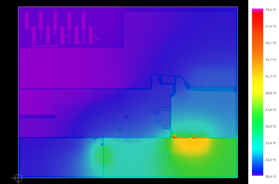
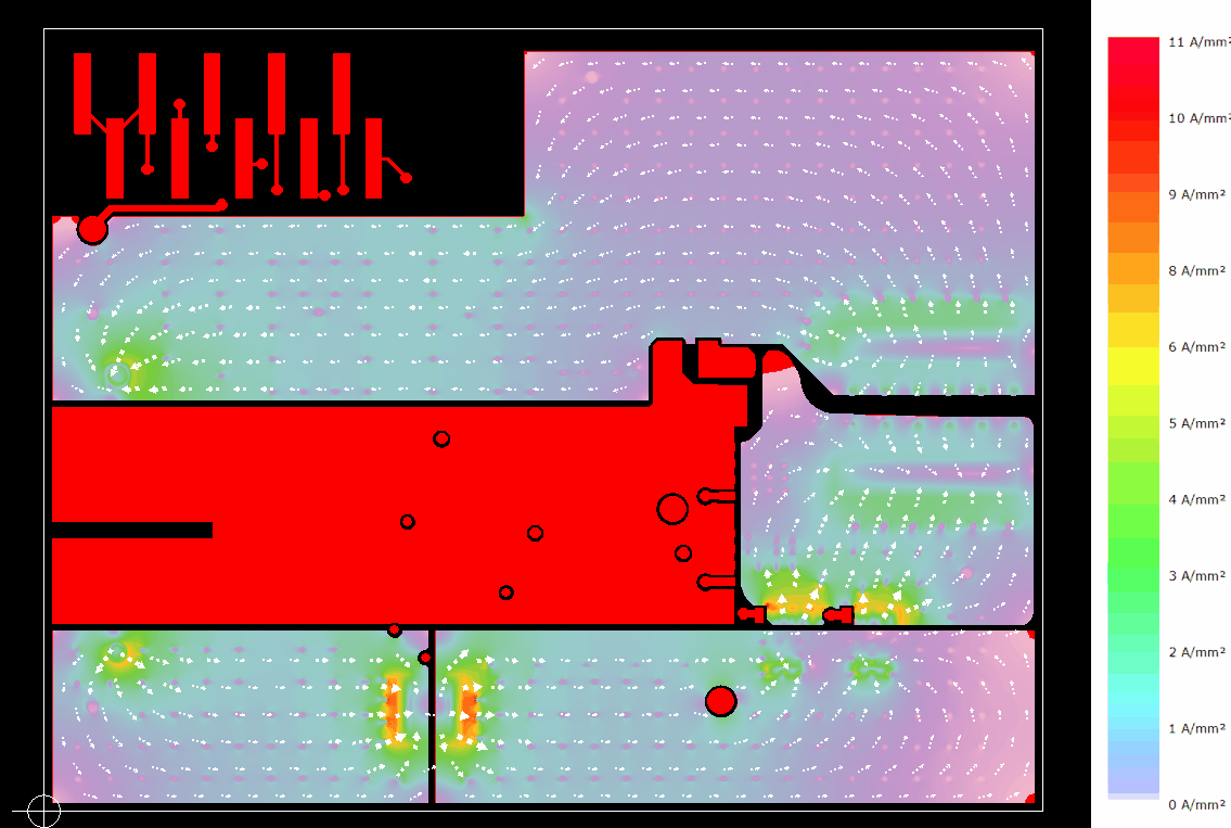
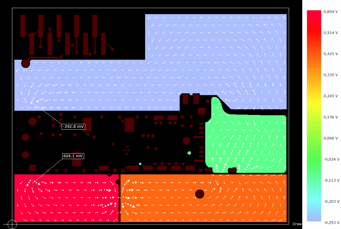
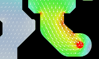
Results: The field solvers calculate values for each simulation point according to raster and layer stack. Base variables are electric potential and temperature. Derived values are current density (vector field), resistance, electric flux and heat flux. The results are accessible by “overlay” plotting on the artwork or in tabular form.
The “Result Viewer” opens automatically when the solution is finished or cancelled.
The last simulation result is automatically loaded, but it is also possible to load former results or import/export results from/to any location
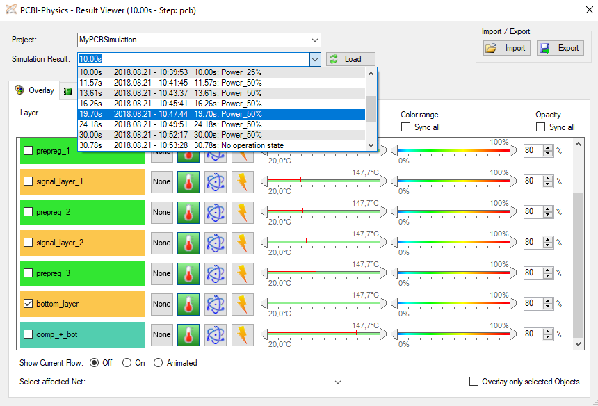
You get a detailed result for every simulation point you have defined.
Default background display is the artwork. Results are additional “overlay data”.
Layer (1):
Activate the layer or prepreg for which you want to see the results. When activating one layer, all other layers are deactivated to keep the clearness. If you really want to display more then one layer including its overlay at the same time, please activate the layers in the normal layer list of PCB-Investigator.
Overlay data (2):
Temperature (°C)
Current density (A/mm²)
Voltage Drop (V)
Value range (3):
By default the overall minimum/maximum values are set. Small red markers show the minimum/maximum values on this layer. You can set minimum and maximum value you want to see in the overlay, e.g. only everything which is hotter than 50°C.
Color range (4):
The range of colors ,which should be used for the selected value range. You can also right click on this slider and then define any value range you want to have.
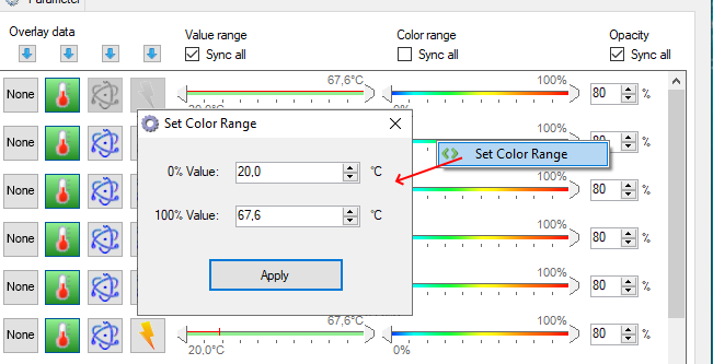
This makes especially sense when comparing two results, e.g.:
By default, red is at 90°C in the first result, and red is at 110°C in second result. But when you define a fix value range from 20°C to 110°C in both cases, colors become comparable, as e.g. yellow will be 70°C in both cases.
Opacity (5):
Saturation of the overlay plot. When defining 100%, the overlay for voltage drop and current density will not be mapped on copper areas only, but will show the real simulated area. There might be a slight mismatch to the CAD copper artwork due to the used raster.
Show Current Flow/ Animation (6):
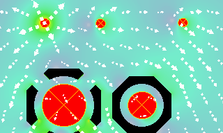
Select affected Net (7):
Select a net or use the mouse wheel to scroll through all nets. The opacity is reduced for all other nets.
Overlay only selected Objects (8):
The overlay is only shown above selected elements/nets, in this way a certain net can be better reviewed.
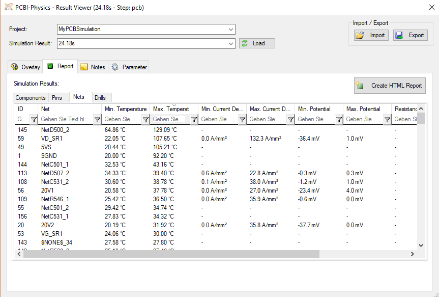
In the report tab, the different simulation parameters and results are shown in following lists. Again, you can select the result for each simulation point (1):
Create HTML Report
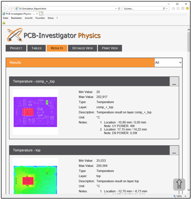
Creates an interactive standalone .html file with all input data, all result data and all plots. The file can be browsed either off-line or distributed by email to team members or customers.
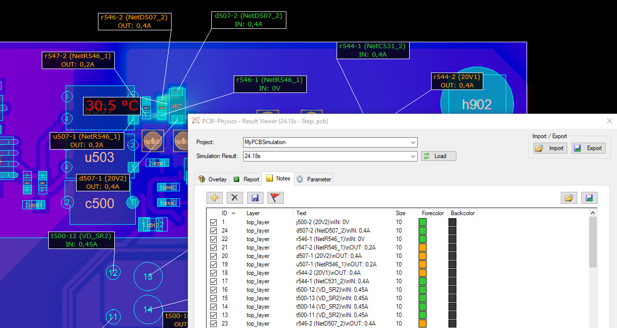
At first you can select the simulation result for a deliberate simulation point. In this tab you can add notes to any location and layer. Notes can contain the overlay value (e.g. 50°C), information about source/sinks or any user defined text. The size and color of each note can be defined by clicking in the corresponding cell in the list. Existing notes can be moved by using Drag & Drop.
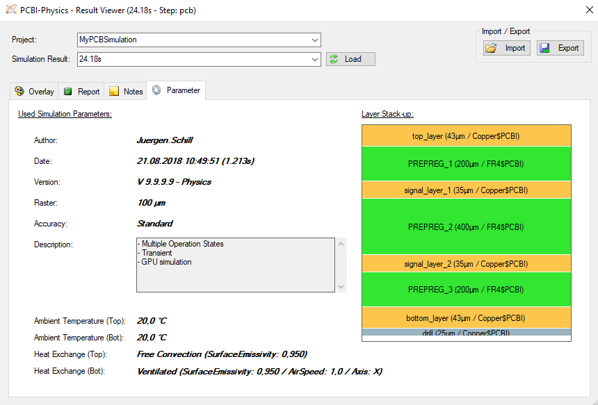
A quick view of basic model parameters used in this simulation. Again, you can view this outline for every simulation point you have defined before.
Procedure in case of a simulation abort:
Watch our PCB-Investigator Physics Videos here:
Tutorial 1: How to use PCB Investigator Physics:
Tutorial 2: Improve thermal behaviour by using different materials:
Tutorial 3: Improve thermal behaviour by optimizing the copper structure of your layout and adding thermal vias:
Tutorial 4: Improve thermal behaviour by adding a Heat Sink to a component with high power dissipation:
Tutorial 5: Improve thermal behaviour by adding an Insulated Metal Substrate (IMS / Aluminum Plate) to the bottom side of the PCB:
Tutorial 6: How to issue time-dependent transient simulations with different simulation states.
Tutorial 7: PinBridges & EasyLogix Par Library