 |
Stencil analysis is used to find undersized soldered pastes. This depends directly on the stencil thickness. |
Before starting the production of a pcb, this analysis` goal is to determine, whether the soldering paste (due to its small surface) can detach from the stencil.
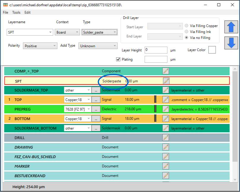
In this analysis only layers are checked, which are defined als soldering paste layers. Looking at the matrix, it is easy to see, which layers are checked here.

1. Ckeck Ratio Rules - If the ratio between the size of the component and the size of the pad is not optimal, this can cause problems when printing the solder paste on the PCB. therefore, you can describe here the ratio between the area of a component and its thickness, and the ratio between the area of an average solder pad and the area of the surrounding solder mask to avoid soldering errors.
Formula for Aspect Ratio = Pad Width (smaller side) / Stencil Thickness
Formula for Area Ratio = Pad Area / Wall Area
2. Check Solder Paste Type Rules - The "Default Ball Rule" states that the size of the solder balls applied to the board should match the size of the pad to which they are applied. The "Round Ball Rule" states that the solder balls on the board should be round to ensure even distribution of solder paste and better solder quality. If the solder ball is smaller than the pad and irregularly shaped, this can cause problems during soldering.
3. Check Pin Gap Rules - This function in Stencil Analysis checks whether the gaps between the pins of a component on the PCB are large enough to prevent short circuits during soldering. If the pin spacing is too small, there is a risk that the solder mask between the pins will break and solder paste will get under the components, which can lead to short circuits or other faults. Control testing can help to detect and correct such problems at an early stage to ensure optimum quality of PCB production.
The result is visible in the Pitch Rule Column, it shows the check value individualy for each component (ser via percent value).
Formula for Distance Percent is Pad Width (smaller side) * given Percent Value
4. Check Metal in Paste Volume Rules - This function checks the ratio between the metal volume and the paste volume (metal-in-paste volume ratio). Excessive metal deposition in the paste volume can impair soldering performance and lead to faults and defects.
5. There are also Option for the Squeegee. You have to mark the "Check Squeegee Direction Rules", it can handle two directions (horizontal and vertical). Depending on your squeegee type it has different distance rules.
6. Check drill in paste. For some drill types it is important to do not have them in the paste, maybe it run away throug the holes. You have only one parameter for an minimum drill diameter, to ignore very small drills.
7. Check MPN Pins. If you have a library connection to e.g. our EPL, you have real pin sizes and positions in the paste pads. With distance checks in all directions you make sure that the placed component is perfectly connected to the PCB.
8. Stencil Distances. Check the stencil opening distance for maximum values in the same network. It is possible for the paste to bond across the copper connection area, so it is recommended to check the distances in the same network.
Note: If you run the distance check and the pin gap rule it is filtered in both groups, we try to do not show double distance issues.
For Squeegee direction Rule it is possiblte to define many rules in the sub dialog:
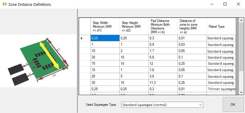
This tool checks the orientation and direction of the squeegee used in the printing process of your circuit board. The tool ensures that the squeegee is aligned correctly to prevent issues such as smudging, misregistration, and insufficient solder paste deposition. The user can define the squeegee direction rules for each component on the board and the tool will check if they are being followed.

The results contain information such as the Area Ratio with an default Ratio = 2.000. To display only the requested results, it is possilble to filter each of the attributes (blue box) shown below using a term (red circle).

Stencil thickness indicates the thickness of the stencil. Since the wall surface of the solder pastes openings determines the thickness of the stencil, it must be selected as thin as necessary and as thick as possible. The thickness of the stencil is an important factor for its longevity, but it negatively affects the adhesion of the soldering paste.
Check only in PCB Profile allows the examination of PCBs across the PCB edge and enables to include the exterior.
In order to secure the results, you can find the option "export"/ "export to file" under the the tab "file" or in the lower right corner. It stores the results in a CSV file.
After saving the stencil analysis result it is possible to add it to the extended design report as table with all important columns.
Each entry has an image of the stencil pad and the connected component, it also has additional information like drill in paste, size and all checked rules.
Here is an example HTML Report:

To have a look on a real html report use this example:
https://www.pcb-investigator.com/sites/default/files/pcbi-demo/DesignReport.html