 |
Using the Component Analysis plugin, you can do a placement and distance analysis for your components, to ensure the manufacturability during your placement and soldering process. This helps to minimize manufacturing costs without affecting product quality, reliability or marketability. |
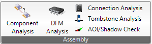
The plugin Component Analysis can be found under the grid "Analysis" respectively "Assembly".
Here you will find two tab pages available for performing the Component Analysis: "Component Distance Analysis" and "Component Placement Analysis". These single analysis functions are described below.
The "Component Distance Analysis" option allows you to check the distance between components and between components and the board outline. This analysis is important to ensure e.g. the manufacturability during the placement and soldering process.
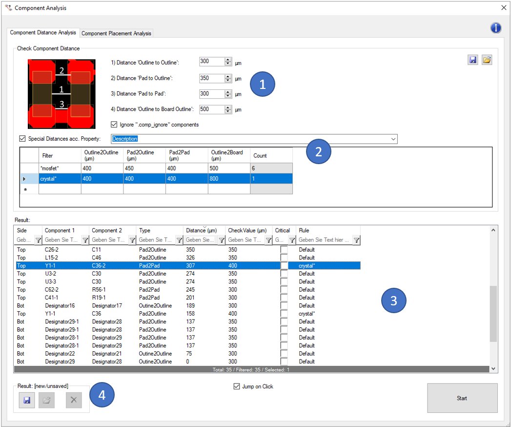
In the first block (1) you can define the different check values:
Here you also have the possibility, to ignore unplaced components (by ignoring components with a ".comp_ignore' attribute).
In the second block (2), you can define "Special Distances acc. Property". That means, you can define the same set of rules as in (1) but with different values for sub groups of components. The Filter is matching a literal string, but wildcards like " * " can be used to make more broad filter settings e.g. 0602*. The sub groups are build by a given component property. Examples are:
The results of the analysis are displayed in the window on the bottom (3). You can also view the analysis results directly in the tool. Critical errors can also be marked for later use (e.g. in the 'Extended Design Report').
With the buttons on the top right side of the window you can export the previously defined settings so that you can reuse them for later analyses. Already saved settings can be imported via the "Import Settings" button.
The last result can be saved and reloaded with the buttons on the lower left side (4). This stored result is also used in the 'Extended Design Report'.
Clicking on the question mark on the top right of the window opens the corresponding page of our online manual.
Following picture shows an example error of this analysis:
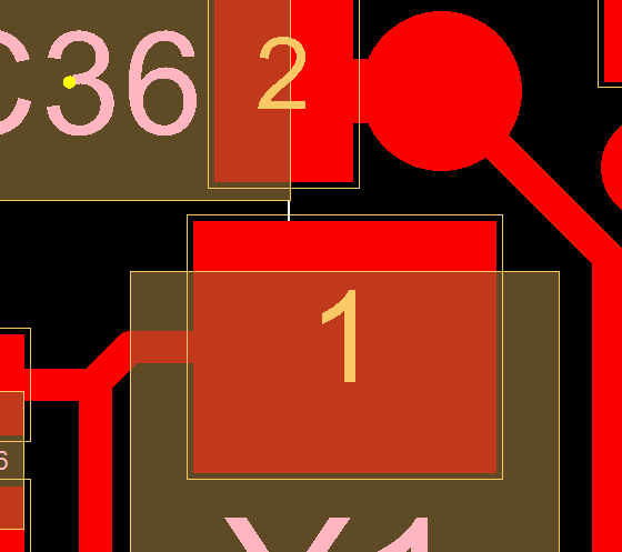
The copper pad of the X1-1 is too close the the component body of C36.
The "Component Placement Analysis" option allows you to check, if the MPN Package of a component fits the CAD Package.
A MPN Package (MPN = Material Part Number) is the real component outline of a part. This outline is often much smaller than the corresponding CAD package body. The MPN Package can also contain the contact surface of the pin. In this analysis, this contact surface of the pins is analyzed. You can define, where the contact surface has to be situated inside the copper pad.
A standard design has no MPN Package definitions included. EasyLogix offers the 'EasyLogix Part Library' (EPL) to add detailed part information like datasheets, MPN packages, 3D step files, ... to your design.
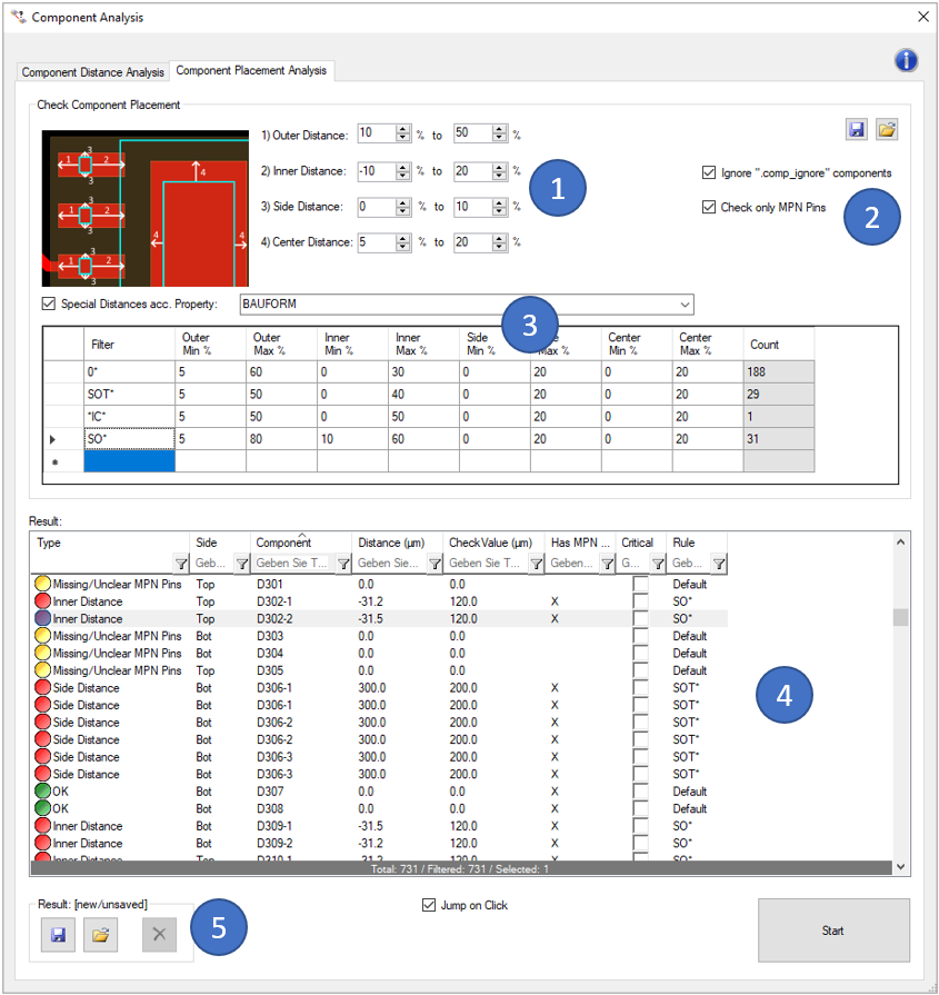
In the first block (1), you can define the different check values:
In the second block (2), you can define filters to ignore unplaced components (by ignoring components with a ".comp_ignore' attribute) and components without MPN package definitions.
In the third block (3), you can define "Special Distances acc. Property". That means, you can define the same set of rules as in (1) but with different values for sub groups of components. The Filter is matching a literal string, but wildcards like " * " can be used to make more broad filter settings e.g. 0602*. The sub groups are build by a given component property. Examples are:
The results of the analysis are displayed in the window on the bottom (4). You can also view the analysis results directly in the tool. Critical errors can also be marked for later use (e.g. in the 'Extended Design Report').
With the buttons on the top right side of the window you can export the previously defined settings so that you can reuse them for later analyses. Already saved settings can be imported via the "Import Settings" button.
The last result can be saved and reloaded with the buttons on the lower left side (5). This stored result is also used in the 'Extended Design Report'.
Clicking on the question mark on the top right of the window opens the corresponding page of our online manual.
Following picture shows an example error of this analysis:
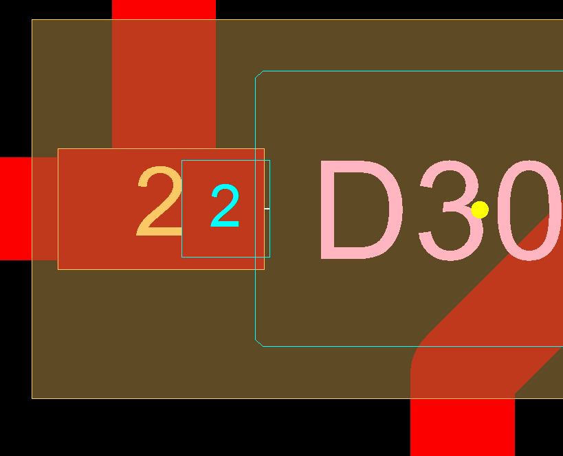
The contact surface of the pin 2 of the MPN Package for D30 is not matching the "inner distance" rule. That means in this case, the pin's contact surface is partly outside the copper pad. A reason could be, that the choosen part (MPN) does not fit to the CAD data. Soldering issues and failures are likely.