

 |
An automated optical inspection (AOI) is an analysis which canvass the solder joints for their correctness after soldering the board. As it is often the case that the camera cannot detect all the components to be inspected, it is necessary to ensure this beforehand. PCB Investigator‘s automated optical inspection provide an analysis tool for this detection of the missing inspectability. |
By using the 'AOI check' button the following window appears:
Example:
Doubleclick an entry shows the component J1 and the corresponding pin 8 (red colored) with too small distance to the component LDR after the 2D inspection.
By using the 'AOI check' button and switching to 3D AOI the following window appears:
Open a PCB design start, then the ‚AOI‘.
3. After you have adapted all values and selection options to your requirements, you can start the inspection
4. The inspected components and their pins are now displayed and can be sorted using the riders. The result list contains one line per pin. It contains the following information:
5. The diagram illustrates the result of the inspection.
6. The inspection can now be saved using the ’Export Result’ option. When using the import result, a past inspection result can be loaded.
7. If you move the mouse over the ’Help’ icon, the following picture will be displayed to explain how 2D inspection works.
8. Ignore components: At this point you have the option exclude components that are not relevant for the later AOI analysis. Depending on your design, you can do this by using the properties, the package name or by individually selecting the components in the tool itself.
Example:
Doubleclick an entry shows the component J1 and the corresponding pin 8 (red colored) with too small distance to the component LDR after the 2D inspection.
By using the 'AOI check' button and switching to 'H-Bridge' the following window appears:
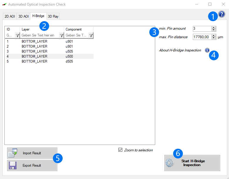
1. If you click on the question mark, you will be redirected to the corresponding page of the manual.
2. ID: Identification Number
Layer: Contains on which side the pin can be found
Component: Component name
3. Min. Pin amount: Minimum number of pins to be checked for an H-Bridge
Max. Pin distance: Maximum distance between two pins up to which a check will be performed
4. By clicking on the "i" you get a short explanation including an illustration showing how the H-Bridge Inspection works.
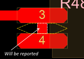
If Copper is found within the marked area, it will be reported during the H-Bridge Inspection. Such areas can cause problems in the later AOI analysis.
5. The inspection can now be saved using the "Export Result" option. When using the "Import Result" option, an old inspection result can be loaded.
6. After you have adapted all values to you requirements, you can start the inspection.
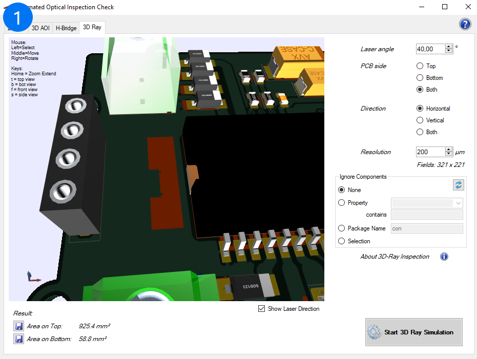
By using the 'AOI check' button and switching to '3D Ray' the following window appears. A 3D model of the PCB to be inspected will be loaded automatically (assuming that the required information on the components is stored in 3D).
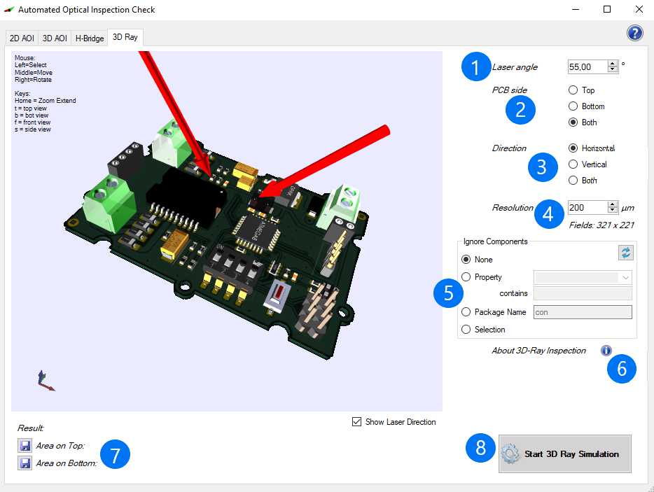
1. Laser angle: Here, you can set the angle at which the lasers should be aligned to the PCB. The changes are also visualized on the model of the PCB.
2. PCB side: Adjustment of the viewing angle (top, bottom, both). Again, you will see the changes of your settings visualized on your 3D model.
3. Direction: Inspection of the PCB in horizontal, vertical (or both) orientation. The new adjustments will be shown on the model.
4. Resolution: Setting of the field size to be considered. The smaller the field, the more accurate the result, but the longer the duration of the simulation (guideline: 200 µm).
5. Ignore components: At this point you have the option exclude components that are not relevant for the later AOI analysis. Depending on your design, you can do this by using the properties, the package name or by individually selecting the components in the tool itself.
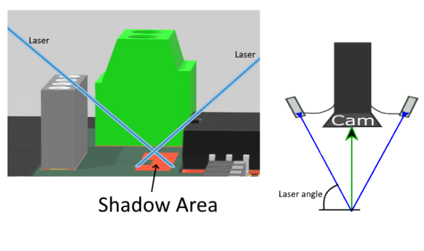
6. If you move the mouse over the 'Help' icon, the following picture will be displayed explaining how the 3D Ray inspection works.
7. By clicking the button "Start 3D Ray Simulation" the simulation starts.
8. You can view the results of simulation in the window on your 3D model (picture 1), in the tool itself (picture 2) or in a list view. The red marked areas show the not inspectable areas. You can then save the results for the top or bottom (or both) side, depending on you default settings. The areas that cannot be inspected will be exactly quantified. Possible changes of the default settings can lead to an improvement (reduction of the not inspectable areas).
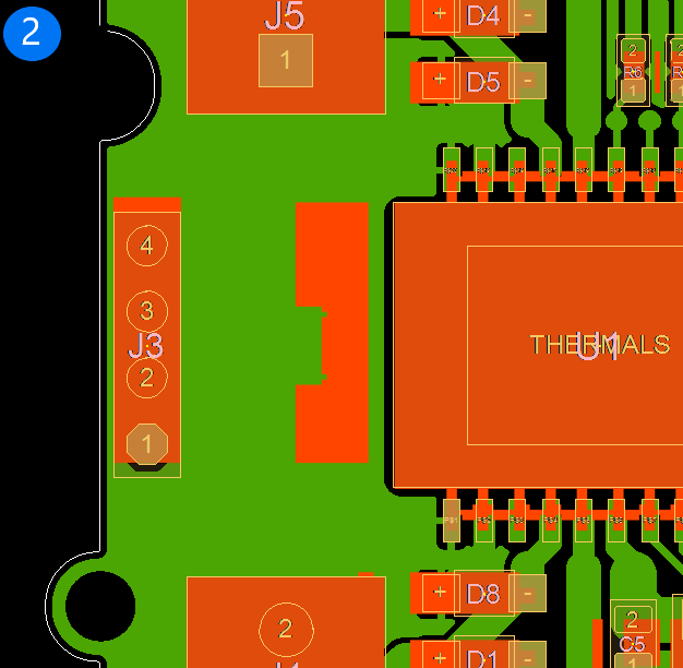
In addition to the visualized representation of the findings, you can also display the results of the simulation in a list view. The list then contains all pins that cannot be inspected by the AOI camera. To show the list, just click on the buttom "Result" on the left corner of the window.
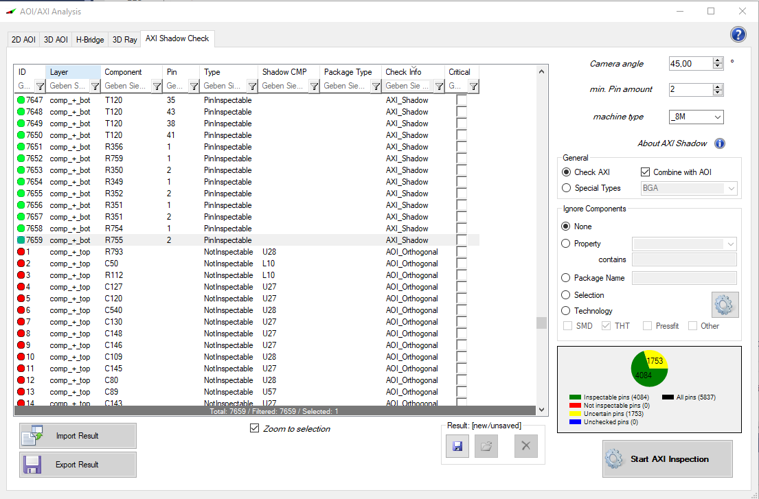
For all AXI machines you can perform the shadow check. This test checks if the material is covered from bottom to top and inverted.
It also supports combination with AOI machines, you have settings for each package type to set the check, e.g. for a chip component it should check only with orthogonal AOI camera, for qfn components with angle camera and for bga all pins checked with AXI analysis.
For each package group you can define the visible pins, hidden pins and material for body and or pins:
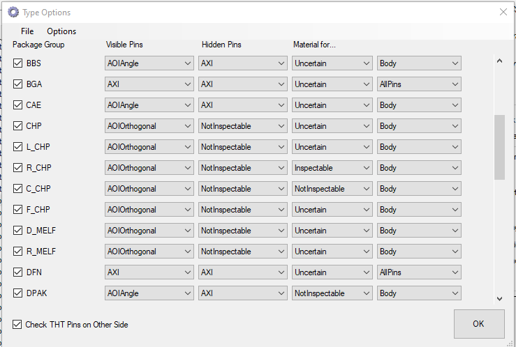
Machine Definition
Each machine has many options to define the cameras, the check methods (AXI, AOI Angle, AOI Orthogonal) with camera angle and the list for all package groups.
If you do not use package groups it use for all the Default rule, this means the visible pins checked by AOI Angle cameras and the hidden pins checked by AXI.
You can handle a list of different machines and use the quick selection in the main dialog to run your analysis directly.
Filter
For all AOI/AXI Analysis checks you can filter for different options like technology (SMD, THT, Pressfit, Other) and properties e.gl Comp Ignore and/or No Pop attribute.
There is also a variant handling option to filter the variant by name.