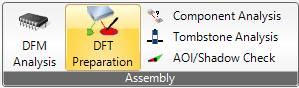
 DFT Preparation is a tool for the easy creation of test programs. So far, machines from Elowerk, Seica, Spea, Takaya and i3070 are supported.
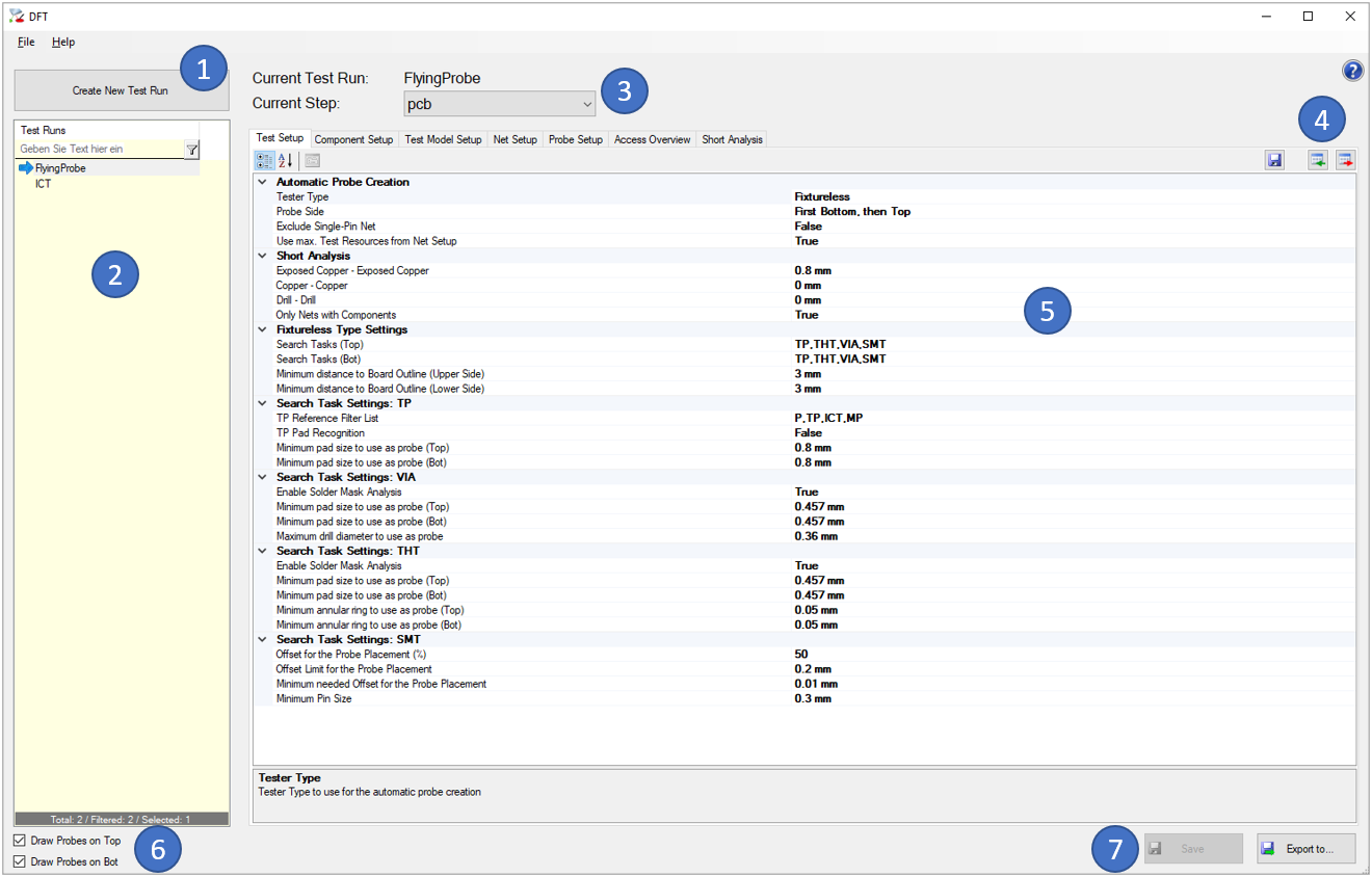
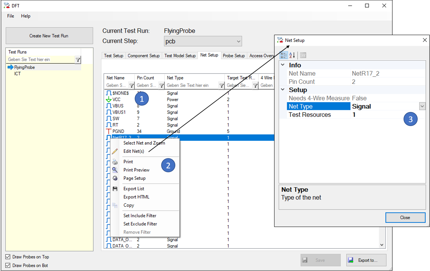
Fixture Parameters:
Tester Type:
Tester Type to use for the automatic probe creation
Probe Side:
Search probes on this/these side(s)
Exclude Single-Pin Net:
Exclude No/Single-Pin Net, all no-pin and single-pin net entries will not create probe entries.
Use max. Test Resources from Net Setup:
If yes, only the given number of Probes are created. If no, all Probes are created
Search Tasks (Top):
Defines the tasks and the order for searching probes on top side
Search Tasks (Bot):
Defines the tasks and the order for searching probes on bot side
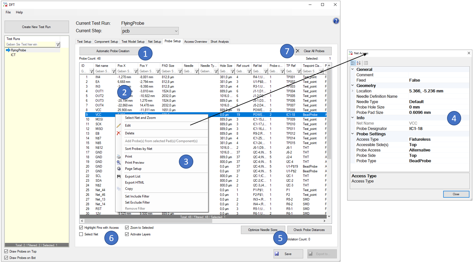
Available Needles:
All allowed needles for fixture probes. Will be used beginning with the largest one. Here also the needed distances to components are defined per needle definition
Standard min. Distance to Components:
If no special distance is defined for the given needle, this is the standard min. distance from probe center to surrounding components
Minimum Distance between Probes:
The minimum distance between Probes, measured from outline to outline (taking diameter of the Needle Definition into account)
TP Reference Filter List:
Comma separated reference filter list (e.g. \"TP, P\"). TP Components must start with one of these entries.
TP Pad Recognition:
Recognize test points by the '.test_point' attribute on copper pads.
Minimum pad size to use as probe (Top):
Minimum copper pad size to create a probe for top side.
Minimum pad size to use as probe (Bot):
Minimum copper pad size to create a probe for bot side.
Enable Solder Mask Analysis:
Enable Solder Mask Analysis, only round pads with openings in solder mask are used if this setting is active.
Minimum pad size to use as probe (Top):
Minimum pad size to create a probe for top side.
Minimum pad size to use as probe (Bot):
Minimum pad size to create a probe for bot side.
Maximum drill diameter to use as probe:
Maximum drill diameter to create a via probe.
Enable Solder Mask Analysis:
Enable Solder Mask Analysis, only round pads with openings in solder mask are used if this setting is active.
Minimum pad size to use as probe (Top):
Minimum pad size to create a probe for top side.
Minimum pad size to use as probe (Bot):
Minimum pad size to create a probe for bot side.
Minimum annular ring to use as probe (Top):
Minimum annular ring to create a probe for top side.
Minimum annular ring to use as probe (Bot):
Minimum annular ring to create a probe for bot side.
Fixtureless parameters:
Tester Type:
Tester Type to use for the automatic probe creation
Probe Side:
Search probes on this/these side(s)
Exclude Single-Pin Net:
Exclude No/Single-Pin Net, all no-pin and single-pin net entries will not create probe entries.
Use max. Test Resources from Net Setup:
If yes, only the given number of Probes are created. If no, all Probes are created
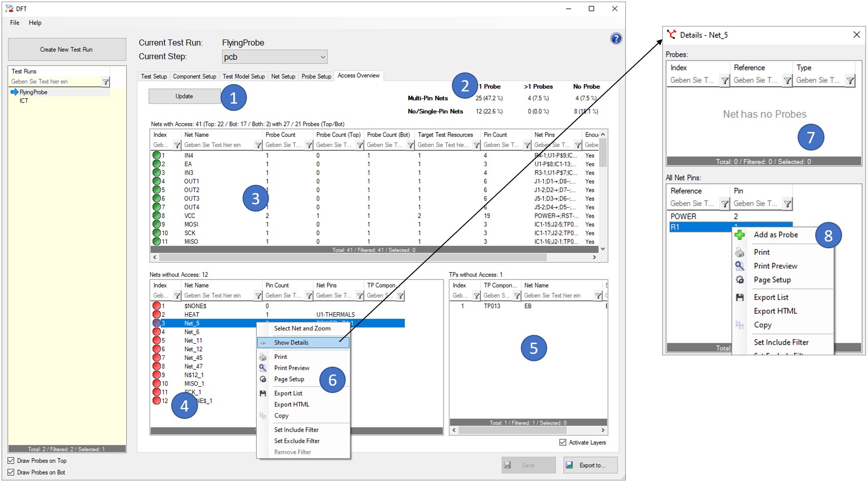
Exposed Copper - Exposed Copper:
The minimum distance between exposed copper areas to not be reported in the Short Analysis (0=deactivated)
Copper - Copper:
The minimum distance between any copper areas to not be reported in the Short Analysis (0=deactivated)
Drill - Drill:
The minimum distance between plated drills to not be reported in the Short Analysis (0=deactivated)
Only Nets with Components:
Only nets with components are checked
Search Tasks (Top):
Defines the tasks and the order for searching probes on top side
Search Tasks (Bot):
Defines the tasks and the order for searching probes on bot side
Minimum distance to Board Outline (Upper Side):
Minimum distance from fixtureless access point center to upper board outline
Minimum distance to Board Outline (Lower Side):
Minimum distance from fixtureless access point center to lower board outline
TP Reference Filter List:
Comma separated reference filter list (e.g. \"TP, P\"). TP Components must start with one of these entries.
TP Pad Recognition:
Recognize test points by the '.test_point' attribute on copper pads.
Minimum pad size to use as probe (Top):
Minimum copper pad size to create a probe for top side.
Minimum pad size to use as probe (Bot):
Minimum copper pad size to create a probe for bot side.
Enable Solder Mask Analysis:
Enable Solder Mask Analysis, only round pads with openings in solder mask are used if this setting is active.
Minimum pad size to use as probe (Top):
Minimum pad size to create a probe for top side.
Minimum pad size to use as probe (Bot):
Minimum pad size to create a probe for bot side.
Maximum drill diameter to use as probe:
Maximum drill diameter to create a via probe.
Enable Solder Mask Analysis:
Enable Solder Mask Analysis, only round pads with openings in solder mask are used if this setting is active.
Minimum pad size to use as probe (Top):
Minimum pad size to create a probe for top side.
Minimum pad size to use as probe (Bot):
Minimum pad size to create a probe for bot side.
Minimum annular ring to use as probe (Top):
Minimum annular ring to create a probe for top side.
Minimum annular ring to use as probe (Bot):
Minimum annular ring to create a probe for bot side.
Offset for the Probe Placement (%):
This parameter is used, if Probes are set to Pins where no TESTPROBE_KEEPOUT but a MPN Package Outline exists. The probe is placed on x % of the distance from the outer edge of the pin to the edge of the MPN Package Outline (also see next parameters). If a keepout is defined, the probe will be placed to the middle of the remaining pin contact area. If no MPN Package Outline is defined, 'Offset Limit for the Probe Placement' is used for the offset.
Offset Limit for the Probe Placement:
This parameter is used, if Probes are set to Pins where no TESTPROBE_KEEPOUT exists. The offset distance calculated with 'Offset for the Probe Placement (%)' is limited to this value, so the offset will not be larger as this value. If no MPN Package Outline exists, this value is used for the offset.
Minimum needed Offset for the Probe Placement:
This parameter is used, if Probes are set to Pins where no TESTPROBE_KEEPOUT but a MPN Package Outline exists. If the offset distance calculated with 'Offset for the Probe Placement (%)' is smaller than this value, no Probe will be placed.
Minimum Pin Size:
Minimum Pin size to be used for the Probe Placement (width and height must be larger/equal
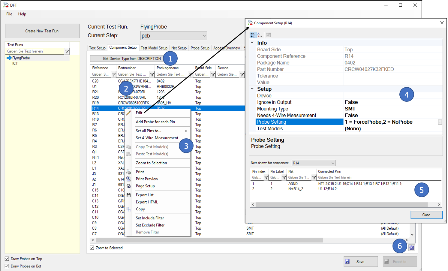
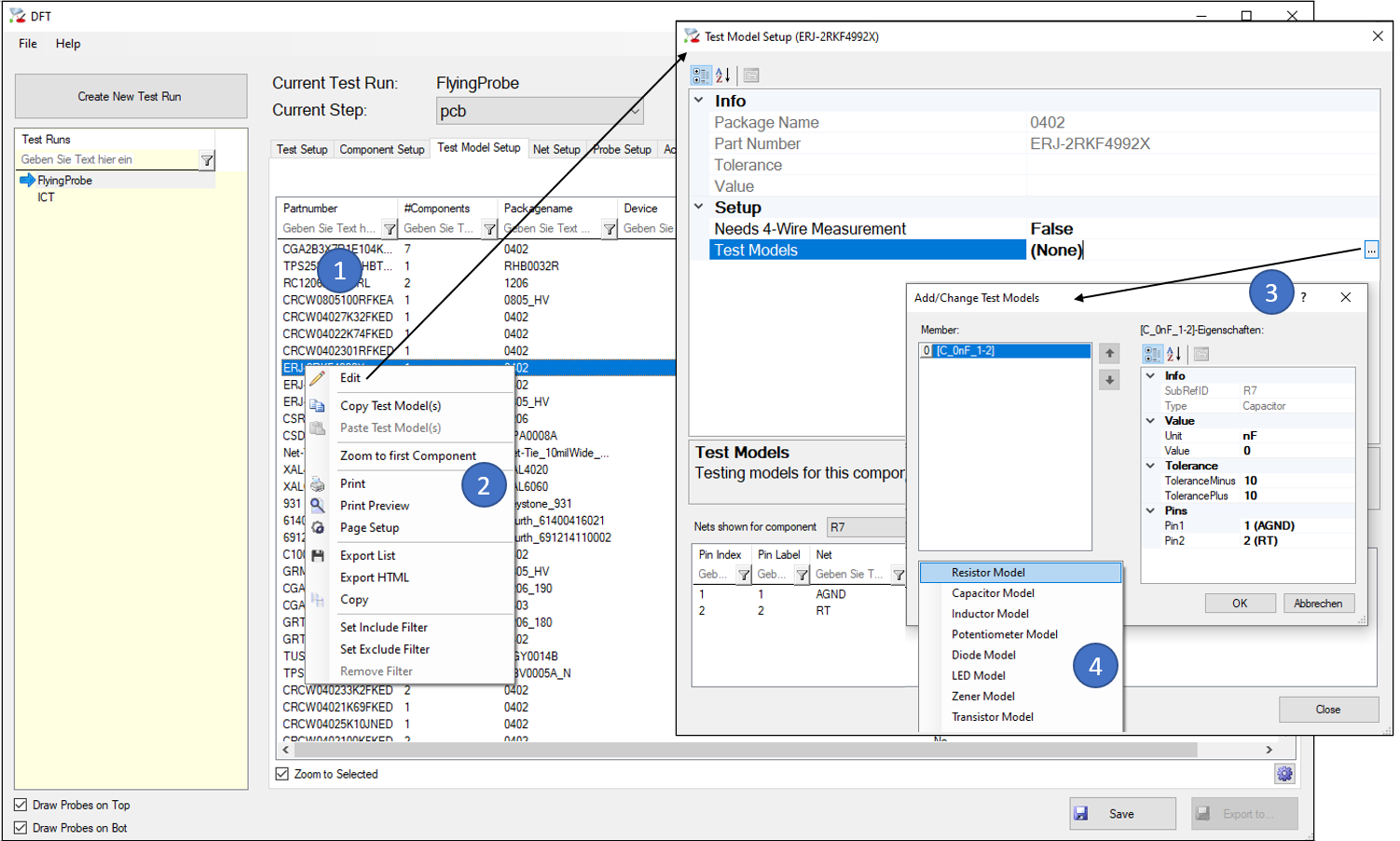
Following test models are available: See appendix.
Additional Rules:
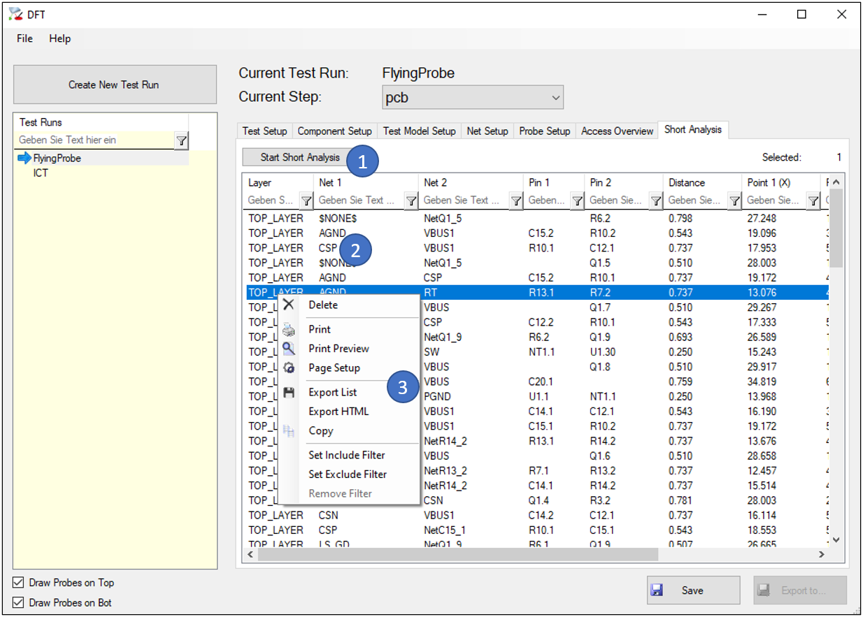
Short measurements will be added in different ways to the exported files:
I3070:
Shorts are not used, as this is a “Fixture” test system
Seica:
Short measurements are exported to the “.shi” file, together with shorts measurements from Pin2Pin test models. Redundancies will be removed first.
Takaya:
Short measurements are exported as Resistor Tests (@K OP). Redundancies with Pin2Pin test models are removed first.
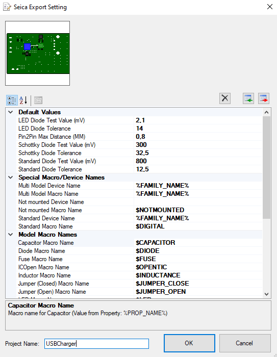
The Seica export creates a package of files (.alf/.inf/.nod/.par/.sha/.shi) that contain all available component and net information to easily create the test program in the VIVA Software of Seica.
Following export settings are possible:
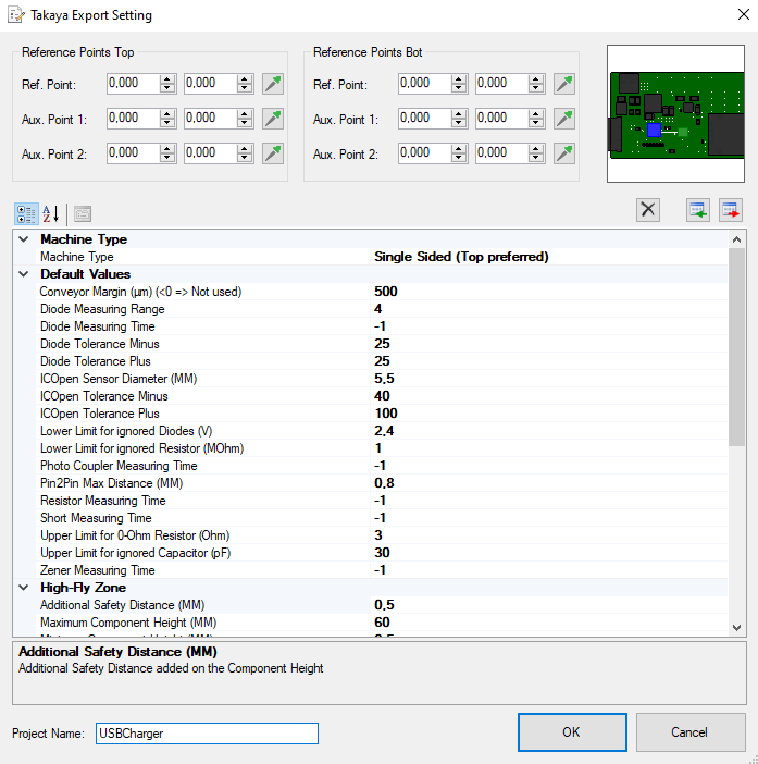
The Takaya export creates a “.ca9” file containing a whole test program. This includes a wire analysis where parallel and serial Resistors/Capacitors/Inductors are merged if there are not enough probes to test them separately. For small value components, that get lost in the tolerance of the overall circuit, additional Vision Tests are created.
The export can be done for one-sided Takaya machines as well as for two-sided ones (4 fingers on one side, 2 on the other).
Following export settings are possible:
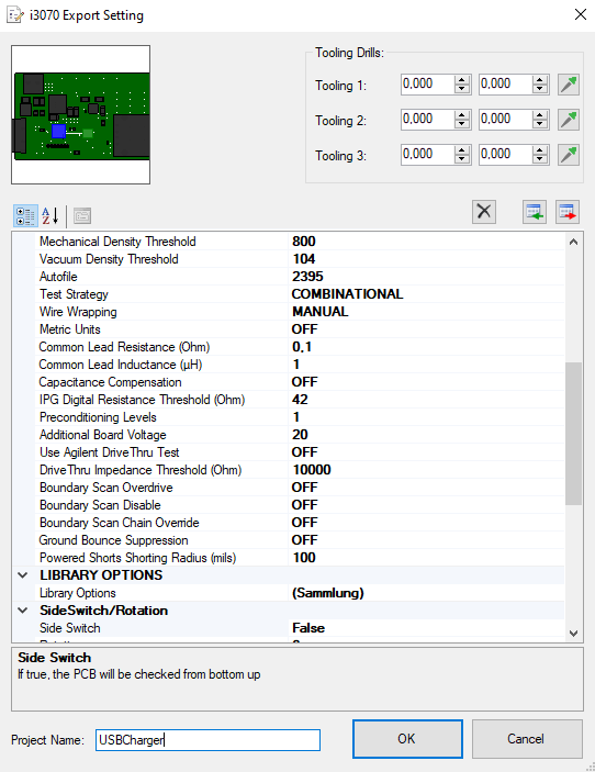
The i3070 export creates a “board” and “board_xy” file that contain all available component and net information to easily create the test program with the native machine software.
Following export settings are possible:
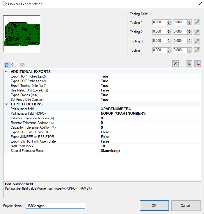
The Elowerk export creates a “xCAM” file that contain all available component and net information to easily create the test program with the native machine software. Optionally also Excellon2 files to create the adapter can be exported.
Following export settings are possible:
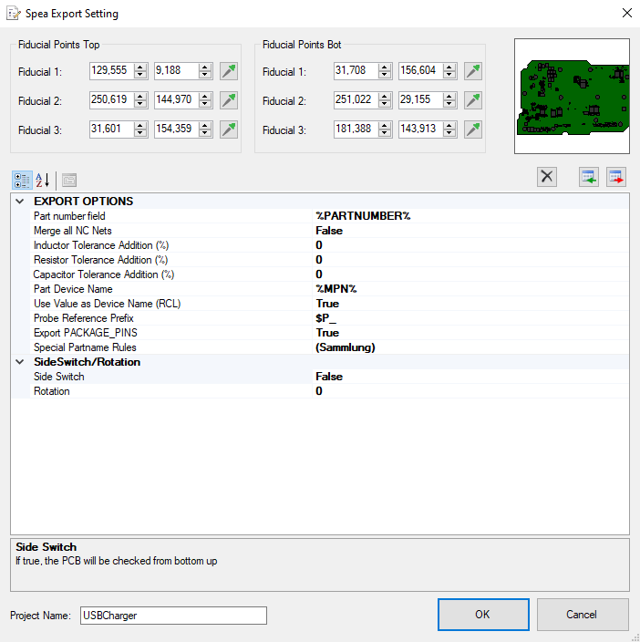
The Spea export creates a “CAD” file that contain all available component and net information to easily create the test program with the native machine software.
Following export settings are possible:
Export tespoint foil as PDF or print it.

The export looks like this:
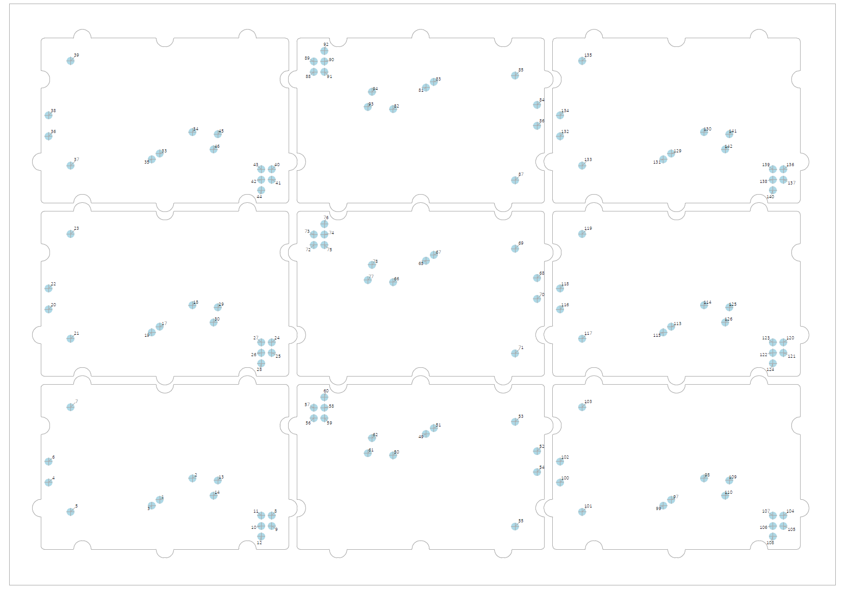
All Labels are searchable in the PDF, for panel it counts up after the first PCB.
| Model | Parameter | Used for Seica | Used for Takaya | Used for i3070 | Used for Elowerk | Used for Spea |
| Resistor | Type | √ | √ | √ | √ (or OTHER if #Pins <> 2) | √ |
| Value | √ | √ | √ | √ | √ | |
| Tolerance | √ | √ | √ | √ | √ | |
| Pins | × | √ | × | √ | × | |
| Capacitor | Type | √ | √ | √ | √ (or OTHER if #Pins <> 2) | √ |
| Value | √ | √ | √ | √ | √ | |
| Tolerance | √ | √ | √ | √ | √ | |
| Pins | × | √ | × | √ | × | |
| Inductor | Type | √ | √ | √ | √ (or OTHER if #Pins <> 2) | √ |
| Value | √ | √ | √ | √ | √ | |
| Tolerance | √ | √ | √ | √ | √ | |
| Pins | × | √ | × | √ | × | |
| Potentiometer | Type | √ | √ (2xResistor) | √ | √ (2xResistor) | √ |
| Value | × | √ | √ | √ | × | |
| Tolerance | × | √ | √ | √ | × | |
| Pins | × | √ | √ | √ | √ | |
| Diode | Type | √ | √ | √ | √ | √ |
| Diode Type | √ | × | × | × | × | |
| Forward Bias | × | × | √ | √ | × | |
| Test Current | × | × | × | √ | × | |
| Pins | × | √ | √ | √ | √ | |
| LED | Type | √ | √ (as Diode) | √ (as Diode) | √ | √ |
| Color | × | √ (2nd Diode Test) | × | × | × | |
| Forward Bias | × | × | √ | √ | × | |
| Test Current | × | × | × | √ | × | |
| Pins | × | √ | √ | √ | √ | |
| Zener | Type | √ | √ (Zener+Diode) | √ | √ | √ |
| Value | √ | √ | √ | √ | × | |
| Tolerance | √ | √ | √ | √ | × | |
| Test Current | × | × | × | √ | × | |
| Pins | × | √ | √ | √ | √ | |
| Transistor | Type | √ | √ (Transistor + 2xDiode) | √ | √ | √ |
| Transistor Type | √ | √ | √ | √ | √ | |
| Pins | × | √ | √ | √ | √ | |
| FET | Type | √ | √ (FET + Diode) | √ | √ | √ |
| FET Mode/Type | √ (only Type) | √ | √ | √ | √ (only Type) | |
| Pins | × | √ | √ | √ | √ | |
| Fuse | Type | √ | √ (4-Wire if possible) | √ | √ (or OTHER if #Pins <> 2) | √ |
| Pins | × | √ | × | √ | × | |
| Jumper | Type | √ | √ (Resistor) | √ | √ (Switch or Resistor) | √ |
| State | √ | √ | √ | √ (Switch) | × | |
| Pins | × | √ | × | √ | × | |
| Switch | Type | √ | √ (Resistor) | √ | √ | √ |
| State | √ | √ | √ | √ | × | |
| Pins | × | √ | √ | √ | × | |
| PhotoCoupler | Type | √ | √ (PhotoCoupler + Diode + Resistor) | √ (PinLibrary) | √ | √ |
| Pins | × | √ | × | √ | × | |
| Seica: Special Model | DIGITAL | √ | × | × | × | × |
| OPENTIC | √ | × | × | × | × | |
| OPENFIX | √ | × | × | × | × | |
| AUTIC | √ | × | × | × | × | |
| VOLTAGEREGULATOR | √ | × | × | × | × | |
| OPAMP | √ | × | × | × | × | |
| COMPARATOR | √ | × | × | × | × | |
| TRIAC | √ | × | × | × | × | |
| SHORTTEST | √ (in the .shi file) | × | × | × | × | |
| Takaya: Special Model | ICOpen | × | √ | × | × | × |
| Pin2Ground | × | √ (Diode Tests) | × | × | × | |
| Pin2Pin | × | √ (Resistor Tests) | × | × | × | |
| i3070: Special Model | PinLibrary | × | × | √ | × | × |
| Connector | × | × | √ | × | × | |
| Elowerk: Special Model | All Types | × | × | × | √ | × |
| Spea: Special Model | All Types | × | × | × | × | √ |
Exceptional cases:
1. If NO model exists
2. If >1 model exists
3. "Not in BOM" is true
General:
- Comment is set to "NOPOP".
- Values are set to "*".
Special:
- Zener: @K is set to F, @MR can be defined, no Zener Test.
- LED: @K is set to F, @MR can be defined, no color test.
- Transistor: @K is set to JP, no Diode Tests.
- FET: @K is set to JP.
- Switch, Jumper, Fuse: @K is set to OP.
- Resistor, Diode, Pin2Ground, Potentionmeter: @K is set to F, @MR can be defined.
- Capacitor: @K is set to E, @MR can be defined.
- Inductor: Esported as Resistor with @K is set to OP, @MR can be defined.
- PhotoCoupler: @K is set to JP/F(Diode)/OP(Resistor).
- ICOpen: @K is set to JP.
General:
- PartNumber is set to "NOPOP".
Special:
- Resistor is exported as Open Jumper.
- Capacitor is exported with 0.1pF.
- Inductor is exported as Open Jumper.
- Transistor is exported with 0.002/0.001V.
- FET is exported with 99999 Ohm.
- Diode/LED is exported with 0.002/0.001V.
- Zener is exported with 0.001V.
- Fuse is exported as Open Jumper.
- Jumper is exported as Open Jumper.
- Potentiometer is exported with 100MOhm.
- Switch is exported "Off".
General:
- PartNumber is created with export option "Part number field (NOPOP)".
- All test models are ignored and the component is exported as "OTHER".
General:
- In the "Part List" section, the "Mounting Side" is set to "P" (not mounted top) or "M" (not mounted bottom).
Watch our PCB-Investigator - DFT Preperation Video here:
Tutorial: DFT Preperation & Machine Export: