To use PCB-Investigator, the software first needs to be installed. To do this, please enter your identification data in your client login first.
All products purchased by you are stored here with downloads, including the license files (floating). You can also access all version updates here, making sure that you always benefit from the latest version of PCB-Investigator.
To stay up to date with our updates, we recommend to subscribe to our newsletter.
After successfully completing the download, you will have access to a zip file containing all the files needed for the installation. To perform the installation, open the .msi file and follow the instructions in the installation wizard. In the additional text file, you will find more information about the installation and possible causes for occurring problems.
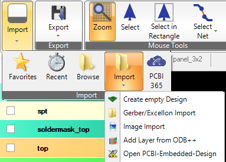
To load a new design or job, click on the “Import” button.
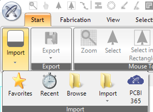
Here, you can choose between
• designs that you have marked as a favorite (“Favorites”),
• recently opened jobs (“Recent”),
• specific files in your data via the “Browse” function,
• an empty design via "Import” or,
• a design via our cloud platform PCB-I 365 (if you are using this service).
Alternatively, you can simply drag & drop your files into PCB-Investigator to open them.
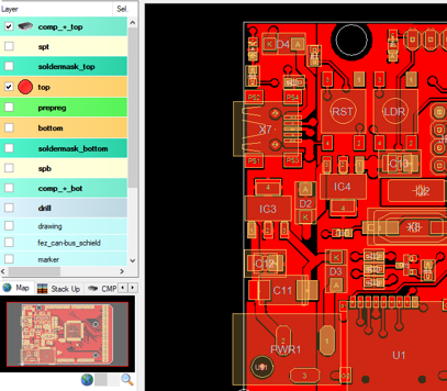
The layer stackup of your currently opened design is displayed on the left side of the main window.
To show or hide layers, check or uncheck the corresponding layer.
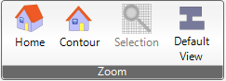
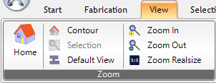
By clicking on "Default View" (under the zoom function in the toolbar at the top), all layers are hidden at once. Only the contour of your design will be visible.
The “Zoom” option allows you to view your design in more detail. The small window below the stackup, showing you a miniature version of your design, serves as an orientation aid. Here, you can see by means of the red rectangle at which point in the design you are currently working.
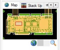
To see or work on specific parts of your design, use the scroll function of your mouse to zoom in towards the corresponding position. You can also use the small window on the left side of the start window to zoom. Simply select the point of the design you want to view more closely by dragging a rectangle to the corresponding position.
If you want to display the design in its original size again, press the "Home" button at the top of the toolbar. Alternatively, you can select "View" in the ribbon above. Likewise, different zoom options are offered here, such as zooming in and out or displaying the "Home" screen showing the full design.
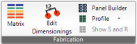
To change the matrix / layer stackup, you have to open the “Fabrication” tools in the above ribbon
to open the matrix.
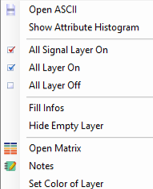
or right-click on the layer stack-up (left side).
The following matrix dialog will open:
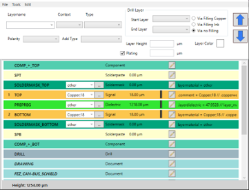
By clicking on the corresponding layer, you can change various parameters of this layer, such as layer name, context, type, layer thickness or polarity. By clicking on the blue arrows on the right side of the window, the position of the selected layer can also be changed by shifting.
To add a layer, click on "Edit" and select "Add Layer" to choose the type of layer. Drill layers are added specifically with "Add Drill Layer".
To save the changes, click on "File" and "Save Matrix". Otherwise, you will be asked to save your changes when closing the window.
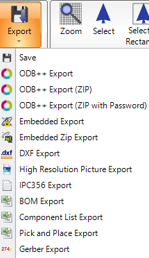
To save changes to a design, select "Export" in the ribbon at the top. You can choose the type of file format, like ODB++, you would like to use to save and export your design. All available file formats PCB-Investigator supports are listed here for you to choose from.
To add data, you can basically use the Import button or drag & drop.
Here, you will find numerous import options. For example, you can use CSV Components to import only components, or additional layers, additional information (attributes), netlists or entire designs.
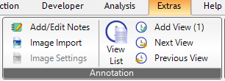
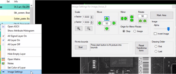
Images can also be loaded via the "Extras" button.
Use the “Image Settings” for adjusting. This serves e.g. the better processing of Gerber files by an enhancement on the basis of illustrations.
To load Gerber files, use the import function or drag & drop analogously to loading other jobs. To be able to fully use Gerber for analyses with PCB-Investigator, we offer you some processing options. To "complete" Gerber files with drill holes, upload the corresponding Excellon file. In addition, the layer stackup needs to be
defined (using the matrix) and possibly, for completion, the components are to be uploaded by means of a CSV file. Deviations in the overlay of layers can be adjusted using "Transform Layers“.
![]()
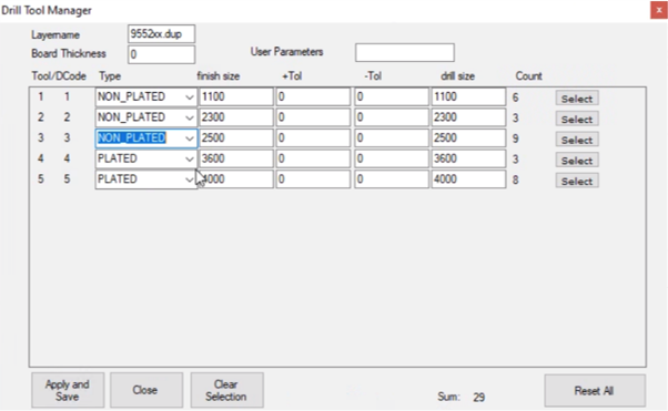
Using the Drill Tool Manager (Right-click on the layer stackup after a drill layer has been selected),
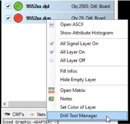
you can define drill holes as plated and unplated (e.g. to perform a DRC analysis).
To import components, you can use the Component (CSV) Import.
This works for all excel or CSV files with References and X/Y positions. If you have only BOM Information you have to use the Part Matcher

The import is easy to use, PCB-Investigator will try to find the columns but user can modify the table indizes manually.
The settings gives you options to identify the packages and place new components with different methodes:

1) options depending to the import table e.g. the unit of X/Y coordinates or the rotation direction (clockwise or counterclockwise).
2) Use existing libraries e.g. the easylogix shared EPackLib to find package outlines and optional part information (with option to set missing packages by part outlines).
3) Package Finder gives many options how to identify the packages, with "Check for Similar Package Names" small nameing differences e.g. 0603C and 0603_C handled identically. Most Important for exising footprint layer is the compare of package footprint with existing pads.

In the Results tab you have some more options:
1) Check each placed package in the Result list, there are markings for Missing/Created and Updated packages
2) Compare with the library, the founded result list (Alternative packages with score) and directly compare all placings in the design
3) Edit the result or replace missing dummy packages with different libraries. You can also create new packages via pad selection with "Create Package from Selection"
Here a short video with the complete workflow:
To view the BOM, use the Component Manager (see Working With Components or here).
To export and print the BOM, use the "Export" tab.

If you want to transfer the components to an other design, you can use the Component List Export and on the other side the CSV Import (see above). But this is only working if you store your package/part definition in an library.
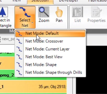
To select nets, click on "Selection" in the bar above. Here, six different selection types for nets will be available. In case of missing net lists (e.g. Gerber files), especially the last two types ("Shape", "Shape through drills") are to be used.
Simply use the left-click to select a net in the graphical interface.
To search for nets, use the search function below the stackup menu on the left side. First, select "Nets". Then enter the corresponding search term to find a net.

This function can additionally be used to track the net structures of your design.
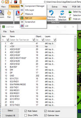
You can also use the Netlist dialog for this purpose. The best way to open it is via the access button on the top of the page (small blue arrow). In the Netlist dialog, you can create a new netlist under "Tools" and "Generate Netlist".
The selection of parts can be performed similarly to the selection of nets using a simple mouse click on the corresponding component in the graphical interface.
The Component Manager gives you access to all components in the design.

The quickest way to open is to click on the small blue arrow in the bar at the top or you access it via the “Extras” tab.
In order to access detailed component properties of any particular part, select a part by clicking on it. Right-click and a small window will open, click on "Properties" and you will get all the part properties (if available in your design or completed by our Easylogix Part Library).

To search for components, proceed in the same way as for the Net search. Switch to the "CMPs" tab in order to carry out a new search for a part in the search bar using the corresponding part name.

Use the PDF Synchronization tool (tab “Extras”) to synchronize or match your design and the corresponding PDF document.

By right-clicking on the respective location (e.g. net or component) in the graphical interface of PCB-Investigator, the associated location within the PDF document will also be highlighted for alignment purposes.
