 |
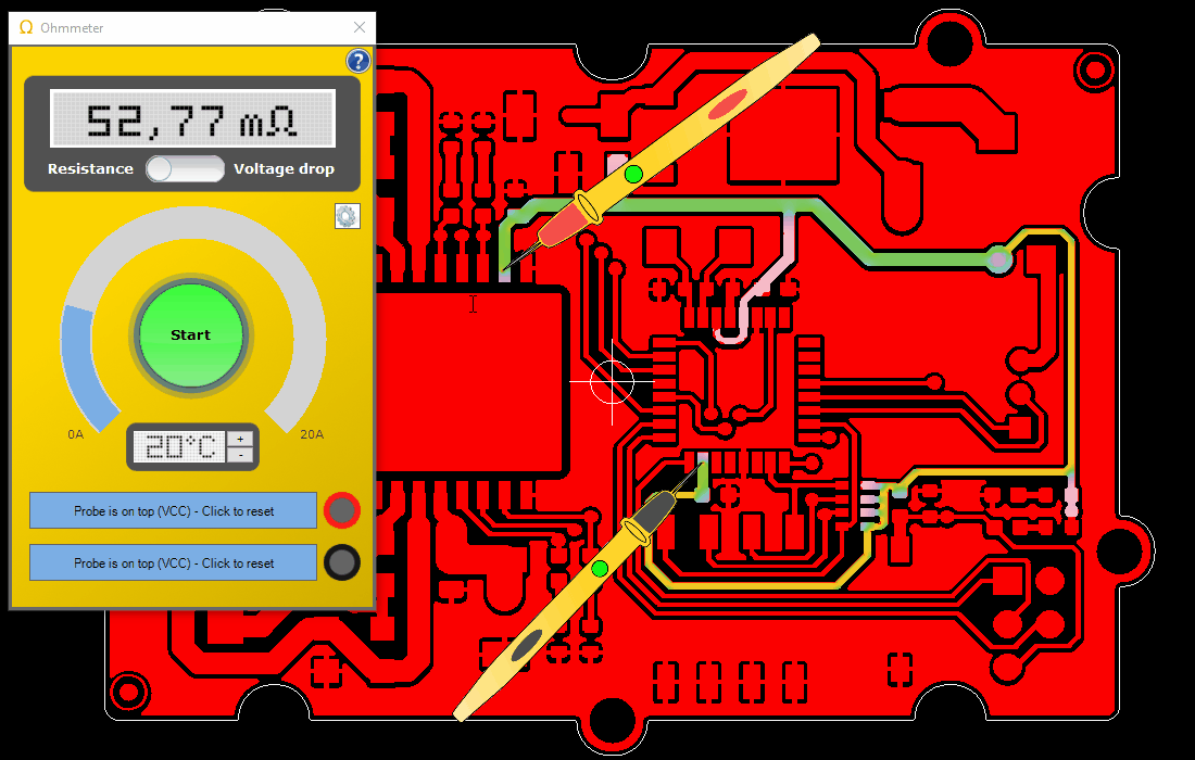
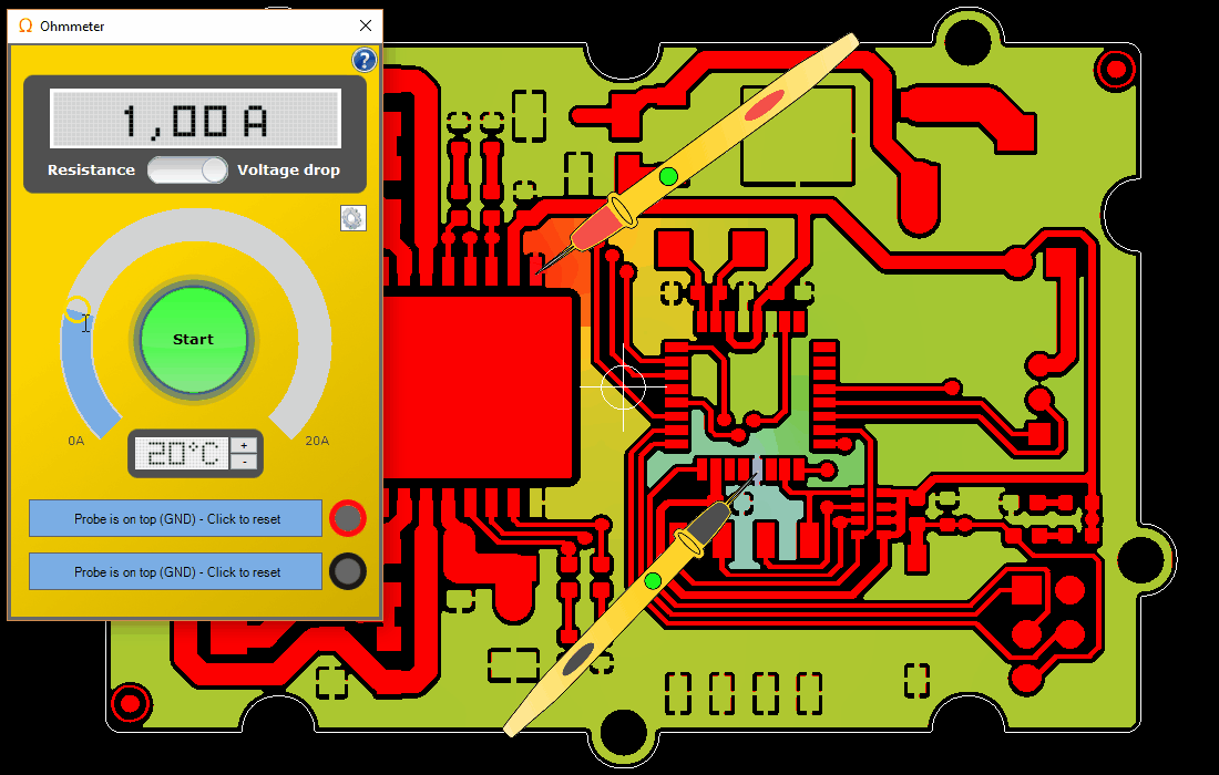
The Ohmmeter of PCB-Investigator Physics enables you to calculate the net resistance and voltage drop between any two points on the PCB. |
The Ohmmeter of PCB-Investigator Physics enables you to calculate the net resistance and voltage drop between any two points of a net on the PCB.
To use the Ohmmeter, you have to define following parameters first:
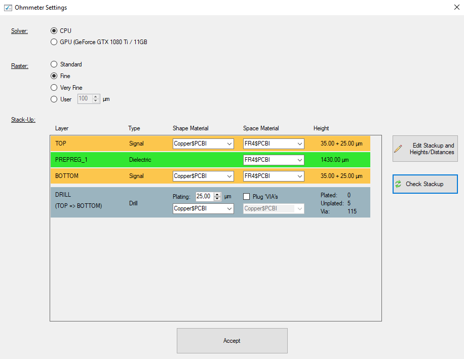
1) Solver:
In most cases calculations run much faster on graphic cards (GPU) than they do on the universal processor (CPU) (from our experience up to 10x faster). But that depends strongly on hardware properties. GPU is only available for recent Nvidia graphic cards with at least CUDA 5.x support. The graphic card should also have at least 2 GB of RAM, better would be 4 or 8 GB.
2) Raster:
The solution requires a large set of nodes inside the PCB volume. Define the spacing in x-y-directions. Standard means a spacing of 0.2 mm, fine 0.1 mm and very fine 0.075 mm. Especially current-carrying traces (only those) need to have at least one, better two, nodes across width. For example the thinnest trace of interest is 0.2 mm wide, then choose at least a raster of 0.15 mm. better take 0.1 mm: The finer the raster, the more computational work. The vertical spacing is defined by the layer stack-up.
3) Stack-Up:
Here you have to define the different materials per layer and the general layer stack-up parameters, especially layer heights.
You can find more details here.
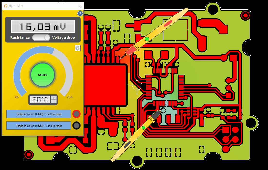
To use the Ohmmeter, please drag the probes with the mouse to the wanted location on the board and drop them there.
The probes can be dropped on different layers, but must be on the same net!
The probes can also be rotated and enlarged by using the mouse.
When both probes are located on the same net, the small green lamps on the probes and the "Start" button in the Ohmmeter are shining green.
Please ensure that the right surrounding temperature of the board is entered in the Ohmmeter dialog and the correct amperes are set (this could be changed by dragging the blue round bar arround the "Start" button with the mouse).
When pressing "Start", the current flow is simulated and the right net resistance is calculated. The result will be displayed in the Ohmmeter. There you also have the possibility to switch between the resistance and the voltage drop.
In the drawing window of PCB-Investigator, you will see the current density overlay or the voltage drop overlay, depending on the switch state.
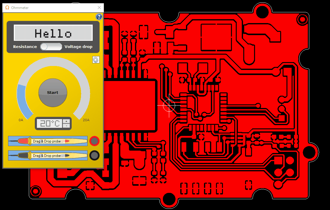
To change the location of the probes, just drag & drop them to the new location, or click on the empty gray space in the Ohmmeter to remove the probes from the board and start from scratch.
Following animations illustrate the use of the Ohmmeter:
1) Drag & Drop the probes and start
2) Move the probes to another net and simulate again. Switch to Voltage Drop.
3) Change the current at the probes
4) Reset the probes, place them on different layers and simulate again