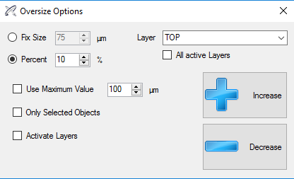
Theoretically, every PCB element can be oversized, but it is arguably most useful utilizing the Oversize function on the soldermask layer. The Oversize function allows you to enlarge each object circumferentially by either a nominal or a percentage value. With especially large objects there also is the possibility to limit the oversize to a fixed µm value. Minimizing is of course also possible. Both variants of the Oversize function, mini- and maximizing, can either be applied to the current selection, each selected, each active, or all layers of the PCB.
A common use case would be ensuring correct margings to counter production-dependent tolerances. If a solder point has the same size defined in your CAD data set as its solder resist recess, it could lead to it being (partially) covered with lacquer in the process of production due to the production-dependent tolerances of 75 µm. Therefore the solder resist mask recesses should circumferentially be larger than the solder pad by 75 µm. If this enlargement wasn\'t already defined in the PCB layout process it can subsequentially be achieved by using the described Oversize function. Furthermore, too small recesses would also be listed as errors while performing a DRC (design role check). PCB-Investigator calls this particular Design Rule Check "Bare Board Check" which is a seperate plugin included in all editions except the Basic one.