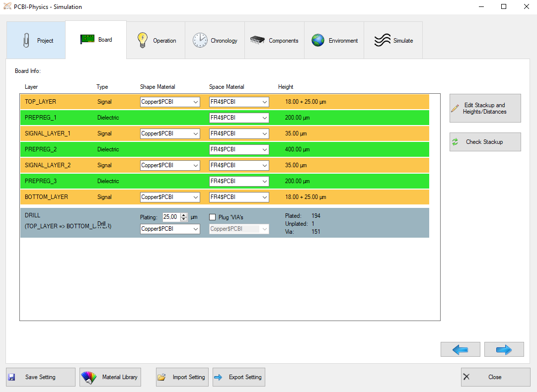
In the ‘Board’ Tab you can check and define the different materials per layer and the general layer stack-up parameters, especially layer heights.
Shape Material:
If the according layer has any CAD elements, the material for those elements can be selected here. Only electrically conductive materials are selectable from the list. For signal layers, “Copper PCBI” is typically the right material. Prepreg layers normally have no CAD elements (Pads, Arefills, Lines, …) on the layer, that’s why this field is hidden. In special cases, also Prepreg layers can contain e.g. a large pad element, which can represent e.g. an embedded copper coin inlay. If such a pad exists, the material for this copper coin inlay can be defined with this field. New materials must be defined in the “Material library” before they can be selected.
Space Material:
The material of empty space on each layer (=area where no CAD elements are) can be defined with this field. Only materials, which are not electrically conductive, are selectable. Typically this is “FR4PCBI”, but also some HighTG Material or even ceramics, glue or other isolation material can be used. New materials must be defined in the “Material library” before they can be selected.
Plating:
The thickness and the electrically conductive material of the plated drill sleeves can be defined for each drill layer. Typically this is 25µm copper. In the simulation model the plating value reduces the end diameter of the hole, so a CAD hole with 300µm and 25µm plating results in a 250µm hole. In ODB++, drill pads can have a property “.drill” with the values “plated”, “non-plated” or “via”. By checking the box “Plug ‘VIA’s”, you can define that all “via” drills are completely filled with the selected electrically conductive material instead of using a conductive sleeve.
Edit Stackup and Heights/Distances:
The layer matrix is opened with this button to add additional layers, change layer heights or reorder the stack-up.
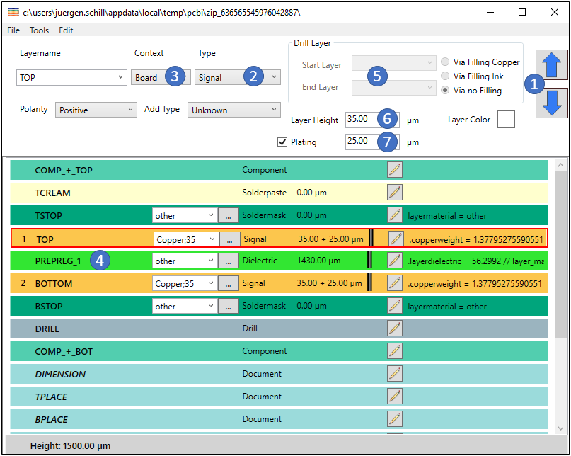
Conditions for a correct stack-up definition:
Important: All other information like “via filling” or material definitions are not used in the simulation and must not be set here!