With the help of the "Rule File Manager" different rule sets can be created and managed.
New:
Create a new rule set with a user defined name.
Save:
Save changes in the currently selected rule set.
Delete:
Delete the currently selected rule set.
Import:
Import a new rule set out of a xml file.
Export:
Export the current rule set to a xml file.
Tolerance:
Tolerance for all check values. All check values will be reduced by e.g. 1% to not show false errors (e.g. when checking for 150µm spacing, a distance of 49.9 µm can be ignored in this way).
Unit Converter:
Small tool to convert numbers between µm and mils.
Compare:
Opens a new window where two rules can be compared in a table view.
Single check rules:
 |
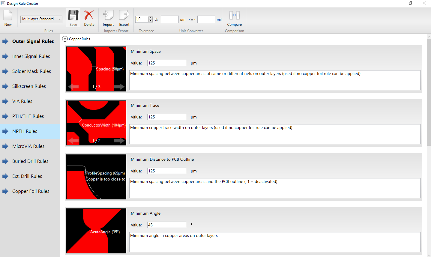
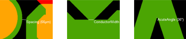
Minimum spacing between copper areas of same or different nets on outer layers (used if no copper foil rule can be applied) |
 |
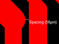
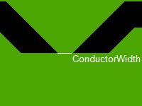
Minimum copper trace width on outer layers (used if no copper foil rule can be applied) |
 |
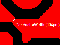
Minimum spacing between copper areas and the PCB outline (-1 = deactivated) |
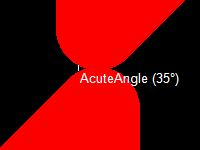 |
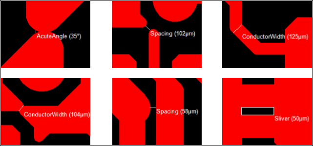
Minimum angle in copper areas on outer layers |
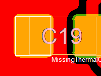 |
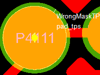
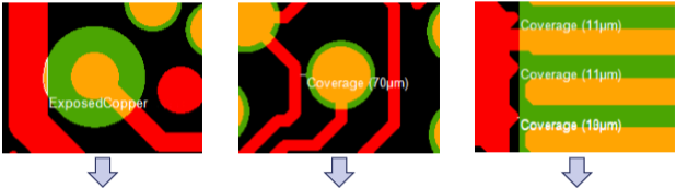
If active, all SMD pads with soldermask opening and component pin are reported, if they are located completely inside a copper area (no thermal reliefs) |
 |
Do not report missing thermal pads, which are located completely under a component body and have a size larger as this value (e.g. cooling pads) |
 |
Minimum needed solder mask clearance arround SMD pads (.smd Attribute) |
 |
Minimum needed solder mask clearance arround test point pads (.test_point Attribute) |
|
Minimum spacing between copper areas of same or different nets on inner layers (used if no copper foil rule can be applied) |
|
Minimum copper trace width on inner layers (used if no copper foil rule can be applied) |
 |
Minimum spacing between copper areas and the PCB outline (-1 = deactivated) |
|
Minimum angle in copper areas on inner layers |
 |
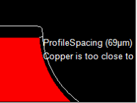
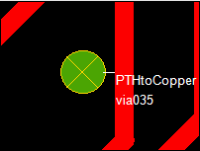
Minimum distance from the solder mask opening to surrounding copper |
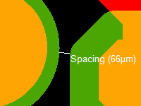 |
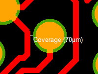
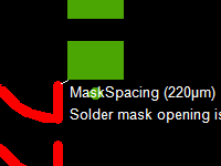
Minimum spacing between solder mask clearances (=smallest solder resist fillet) |
 |
Minimum width of solder mask clearances |
 |
Minimum angle in solder mask clearances |
 |
Minimum distance to any solder mask opening |
 |
Minimum distance to any component |
 |
Check only text primitives (.nomenclature attribute) for a minimum distance to components, or all primitives |
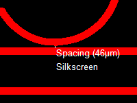 |
Minimum spacing between silkscreen printings |
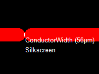 |
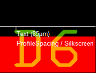
Minimum size of silkscreen primitives |
 |
Minimum spacing between silkscreen printings and the PCB outline (-1 = deactivated) |
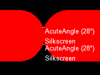 |
Minimum angle in silk screen printing |
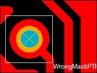
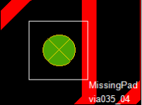
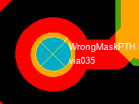
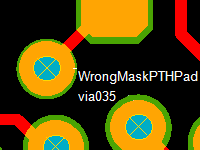
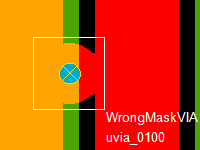
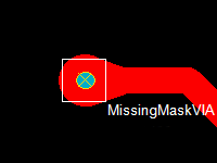
| Minimum needed solder mask clearance for plated through holes (.drill=via) |
| Minimum needed solder mask clearance for plated through hole copper pads (.drill=via) |
 |
If active, mask clearances which are smaller than the VIA-Pad are not reported |
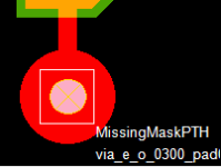 |
If active, missing solder mask openings for VIA drills will not be reported |
|
If active, missing solder mask openings for VIA drills will not be reported |
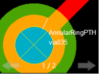 |
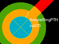
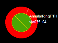
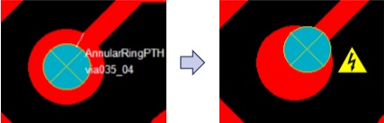
Minimum annular ring for the VIA on outer signal layers |
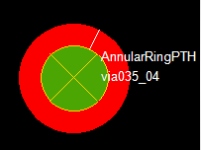 |
Minimum annular ring for the VIA on inner signal layers |
 |
If active, missing copper pads on inner signal layers will not be reported |
 |
Minimum distance to surrounding copper on inner layers, if missing pads are accepted |
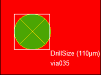 |
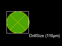
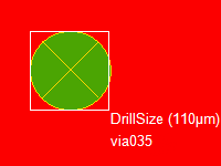
Minimum diameter of plated through holes (.drill=via) |
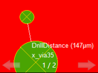 |
Minimum Distance to any other Drill |
 |
Minimum needed solder mask clearance for through hole technology drills (.drill=plated) |
 |
Minimum needed solder mask clearance for through hole technology copper pads (.drill=plated) |
 |
Minimum annular ring for the through hole technology drills on outer signal layers (.drill=plated) |
 |
Minimum annular ring for the through hole technology drills on inner signal layers (.drill=plated) |
 |
If active, missing copper pads on inner signal layers will not be reported |
 |
Minimum distance to surrounding copper on inner layers, if missing pads are accepted |
 |
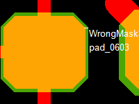
If active, all THT copper pads are reported, if they are located completely inside a copper area (no thermal reliefs) |
 |
Minimum diameter of through hole technology drills (.drill=plated) |
 |
Minimum Distance to any other Drill |
 |
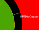
Minimum needed solder mask clearance for unplated through holes (.drill=non_plated) |
 |
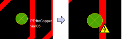
Minimum distance to surrounding copper on outer signal layers |
 |
Minimum distance to surrounding copper on inner signal layers |
 |
Minimum diameter of unplated through holes (.drill=non_plated) |
 |
Minimum Distance to any other Drill |
 |
Minimum needed solder mask clearance for laser drills |
 |
If active, missing solder mask openings for laser drills will not be reported |
 |
Minimum annular ring for the laser drill on all affected signal layers |
 |
Minimum diameter of laser drills |
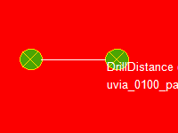 |
Minimum Distance to any other Drill |
 |
Minimum annular ring for the drill on outer signal layers |
 |
Minimum annular ring for the drill on inner signal layers |
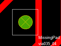 |
If active, missing copper pads on inner signal layers will not be reported |
 |
Minimum distance to surrounding copper on inner layers, if missing pads are accepted |
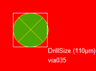 |
Minimum diameter of plated through holes |
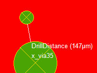 |
Minimum distance to any other Drill |
|
Minimum Distance from THT to THT Drill |
|
Minimum Distance from THT to VIA Drill |
|
Minimum Distance from THT to NPTH Drill |
|
Minimum Distance from THT to MicroVIA Drill |
|
Minimum Distance from THT to Buried Drill |
|
Minimum Distance from VIA to VIA Drill |
|
Minimum Distance from VIA to NPTH Drill |
|
Minimum Distance from VIA to MicroVIA Drill |
|
Minimum Distance from THT to Buried Drill |
|
Minimum Distance from NPTH to NPTH Drill |
|
Minimum Distance from NPTH to MicroVIA Drill |
 |
Minimum Distance from NPTH to Buried Drill |
|
Minimum Distance from MicroVIA to MicroVIA Drill |
 |
Minimum Distance from MicroVIA to Buried Drill |
|
Minimum Distance from Buried to Buried Drill |
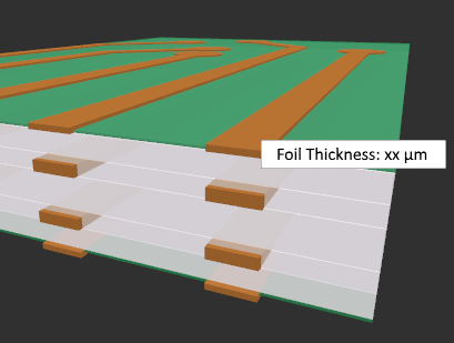 |
Maximum Foil thickness for this rule |
|
Minimum spacing between copper areas of same or different nets on outer layers with this foil |
|
Minimum copper trace width on outer layers with this foil |
|
Minimum spacing between copper areas of same or different nets on inner layers with this foil |
|
Minimum copper trace width on inner layers with this foil |
The result explanations help you to easily interpret the check results reported by PCB-Investigator`s Design Rule Check.
There is a focus on illustrating the technical background as well as on giving a understanding of the unavoidable tolerances during the PCB manufacturing process.
Small distances in copper, as well as thin copper areas might not be producible due to physical etching restrictions.
A chosen technology e.g. IPC Class II should be applied everywhere on the board, as only a single violation forces the PCB supplier to switch to finer production parameters (e.g. IPC Class I) for the whole board.
The finer the structures, the more expensive the board will be.
Solder resist webs with a width of less than app. 70µm are hardly producible with standard technology.
There is always the risk, that those small pieces will detach and adhere somewhere else, which can lead to solder problems and failures.
Smaller distances and webs might only be producible with an expensive special solder resists and less resist height, which influences the isolation quality.
To avoid unnecessary costs, PCB-Investigator reports all those violations.
 CAD data
 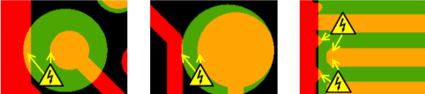 With allowed displacement
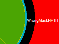
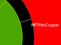
 As there will always be a slight displacement between the solder resist and the conductive pattern, surrounding copper should have a minimum distance of the allowed displacement from the solder resist opening. If not, there is the risk that the surrounding copper will also be exposed, which can lead to electric shorts by e.g. solder bridges.
The allowed displacement is app. 75µm, also 50µm is possible, but more expensive.
 CAD data
  With allowed displacement
 The displacement can also have negative impact on the solderability of SMD pads or testability of test points.
To ensure further processability, there should be a solder resist opening with an oversize of the maximum allowed displacement (e.g. 75µm) for all SMD pads and test points.
So, the copper will always be completely solderable/testable.

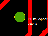
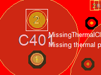
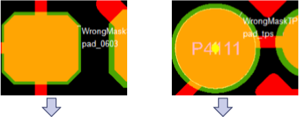
Each drill should have a solder resist opening, which ensures that the drill is free of solder resist despite the combined displacement of the solder resist and of the drill itself.
A partly covered drill or solder resist in the drill sleeve can detach and adhere somewhere else during the cleaning process. This can lead to solder problems and failures and contaminates the chemical baths of the PCB supplier. It also effects the EMC behavior.
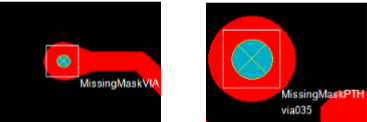
A completely covered drill without any solder resist opening on one side can´t be cleaned and therefore contaminates the chemical baths.
If covered on both sides, the enclosed air in the drill could break the solder resist cover when expanding due to heat. The result is unwanted dirt on the board.
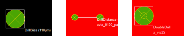
The drill diameter and the drill distance are very important factors for the price calculation.
Very thin drills have a short life period and must often be replaced. They are also less long, which forces the PCB supplier to drill only 1-2 panels at the same time instead of drilling e.g. 5 panels in a package.
Small distances between two drills increase the risk the drill is breaking or the two holes are merging to one undefined shape.
Two holes at the same location can also lead to broken drills or an undefined hole shape.
To achieve a clearly defined connection between layers, the copper pads for the single drills must be large enough, so that a drill displaced within the allowed tolerances is still located completely within the pad.
If not, this can have a strong impact on the EMC behavior and lead to failures due to a loose or broken contact.
Small annular rings and therefore narrow tolerances in the drilling process might still be producible, but force the PCB supplier to use high-end drilling machines and to drill only one Panel at the same time instead of e.g. 5 panels in a package. This has a very strong influence on the PCB costs.
In this case we must differ between plated and un-plated drills.
For plated drills, the distance to surrounding copper is important on inner layers, when the copper pad is omitted. Due to the production tolerances, the displacement of the drill could lead to broken connections or shorts, if surrounding copper is too close.
For unplated drills, the distance is needed for tenting the hole during the plating process to avoid copper in the hole. When the un-plated drill could not be securely tented, a second drill process after the plating process is needed instead. This raises the costs enormously.
Summary
Performing the Design Rule Check (DRC) of PCB-Investigator is the first step to avoid unneeded costs and to increase the reliability of your PCB.
Although in some cases the standard rules must be violated to fulfill some requirements (e.g. Space requirements), there is always a potential to save money and increase the reliability with a few minor layout changes.
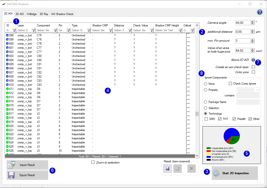
By using the 'AOI check' button the following window appears:
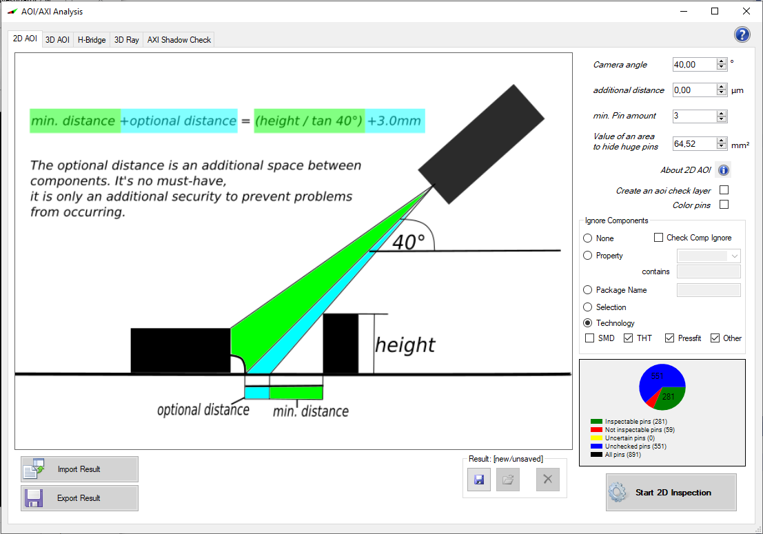
Example:
Doubleclick an entry shows the component J1 and the corresponding pin 8 (red colored) with too small distance to the component LDR after the 2D inspection.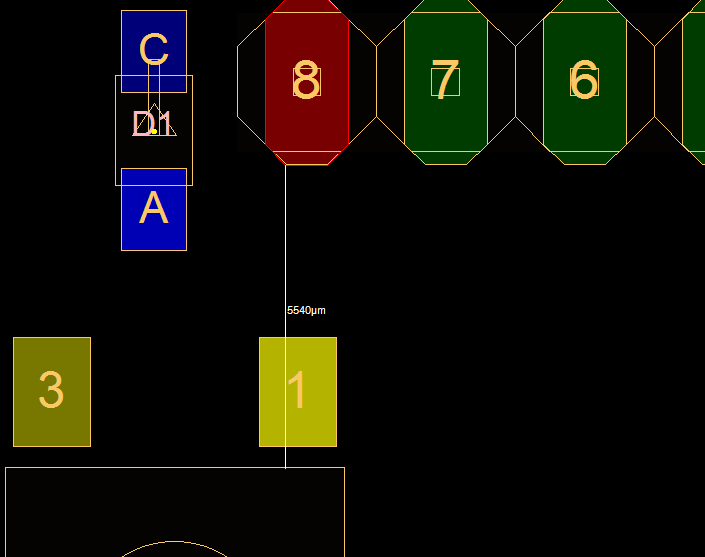
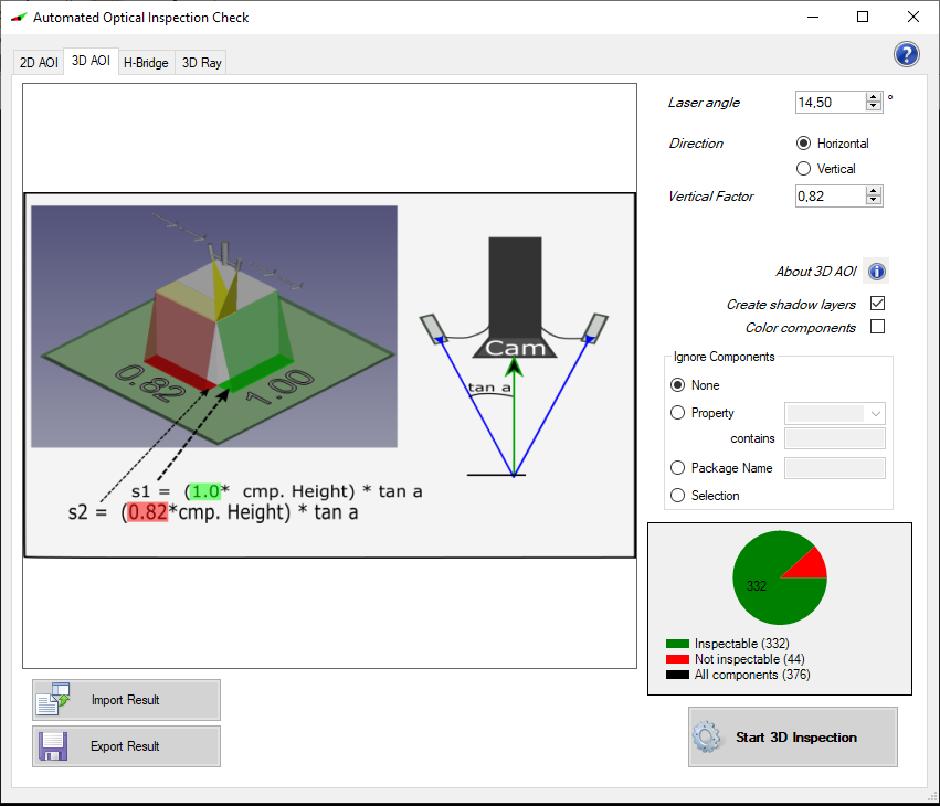
By using the 'AOI check' button and switching to 3D AOI the following window appears:
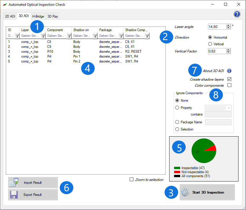
Open a PCB design start, then the ‚AOI‘.
3. After you have adapted all values and selection options to your requirements, you can start the inspection
4. The inspected components and their pins are now displayed and can be sorted using the riders. The result list contains one line per pin. It contains the following information:
5. The diagram illustrates the result of the inspection.
6. The inspection can now be saved using the ’Export Result’ option. When using the import result, a past inspection result can be loaded.
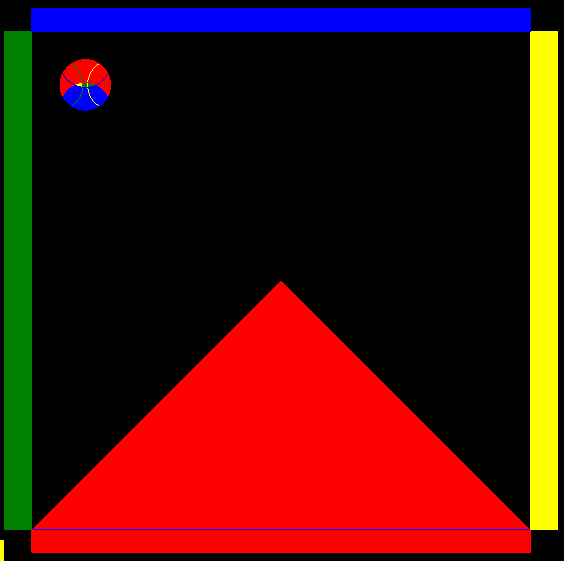
7. If you move the mouse over the ’Help’ icon, the following picture will be displayed to explain how 2D inspection works.
8. Ignore components: At this point you have the option exclude components that are not relevant for the later AOI analysis. Depending on your design, you can do this by using the properties, the package name or by individually selecting the components in the tool itself.
Example:
Doubleclick an entry shows the component J1 and the corresponding pin 8 (red colored) with too small distance to the component LDR after the 2D inspection.
In addition to the distance calculation, an area calculation following the risk assessement tool of ZVEI is also supported.
Settings
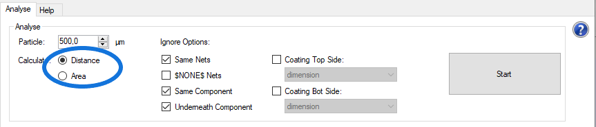
Important type of test (Calculate Distance):
Examining, it is necessary to distinguish, which areas should be examined together. The two types of simulating shown here differ mainly in the speed of test and their accuracy (number of results found).
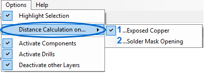
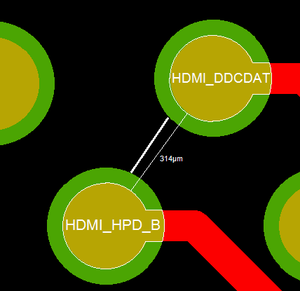
1. Choosing "Exposed Copper", the non-lacquered (omitted), conductive copper pads and copper lines are compared directly to each other. This type of simulation takes a bit longer, but produces significantly more precise results (thin white line).
2. Choosing "Solder Mask Opening", it isn´t the direct copper pads or copper lines that are used for comparison, but the so called solder mask openings, i.e. the surfaces not being covered with varnish. However, these are slightly larger than the copper areas they release (thick white line).
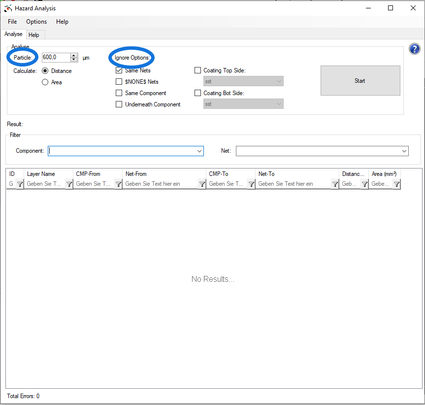
Particle:
The length of the assumed contamination can be parameterized here.
Ignore Options:
1. If the contamination is located between elements of the same net, you can select whether the entries should be ignored or not.
2. If you select the option "underneath component", results of possible short circuits being completely under components will be hidden.
3. If the option "same component" is activated, possible short circuits between pins of the same component will be hidden.
4. If nets are connected by contamination and at least one of the nets is a not-used "$NONE$" net, the results can be hidden as well.
5. You can also ignore areas with coating (Top oder Bot side). The coating prevents the occurrence of short circuits. Therefore these areas are not relevant for the analysis. For a quick calculation use layers with surfaces for the covered areas, all copper below the coating surfaces will be ignored for further calculations.
Filter options:
Filter:
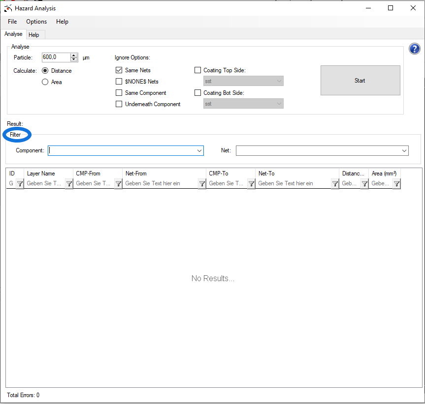
If you want to look closer at a certain component or net, you can filter by using the two drop down menus. In this case, the list is filtered to only show the selected net or component (either in the 'from' or the 'to' column).
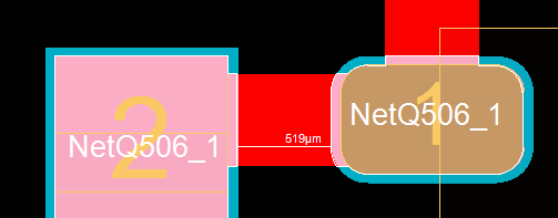
Example Area Calculation:
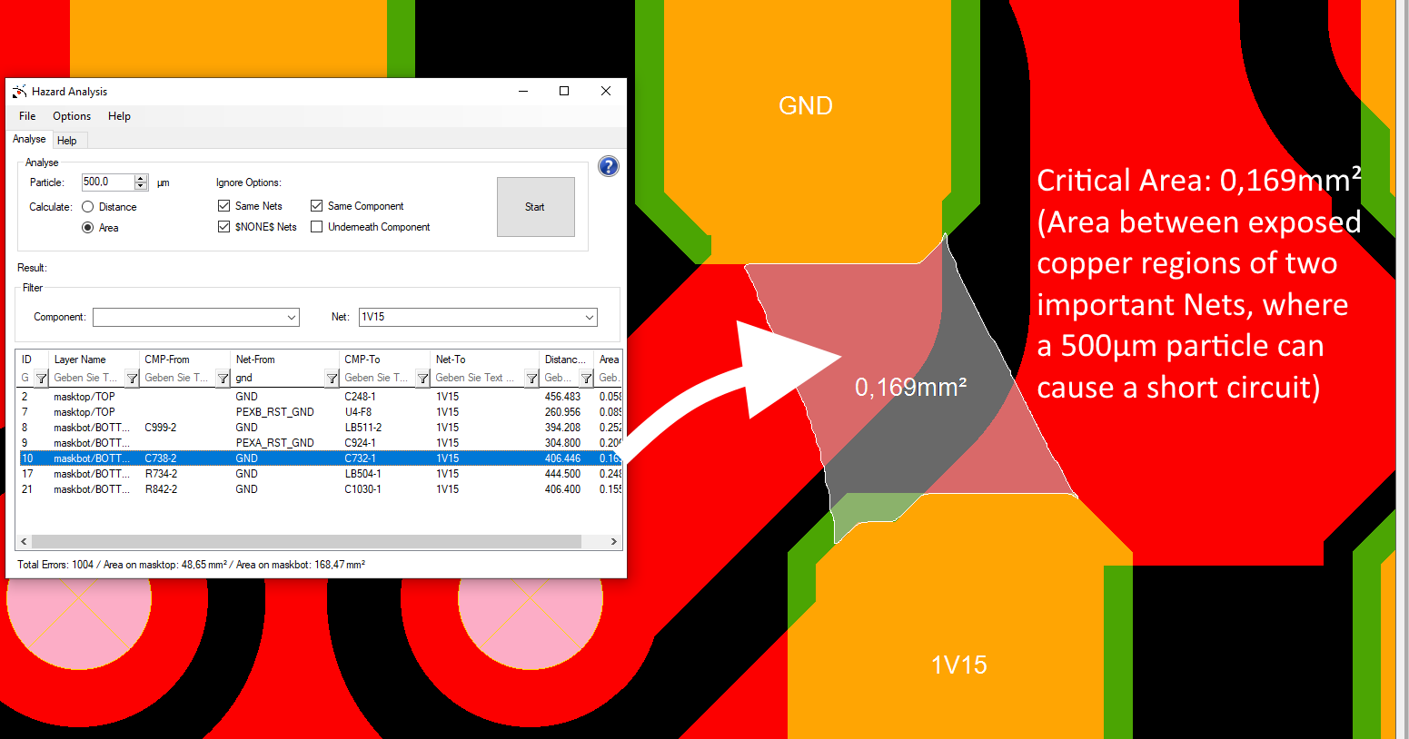
Before starting the production of a pcb, this analysis` goal is to determine, whether the soldering paste (due to its small surface) can detach from the stencil.
In this analysis only layers are checked, which are defined als soldering paste layers. Looking at the matrix, it is easy to see, which layers are checked here.

1. Ckeck Ratio Rules - If the ratio between the size of the component and the size of the pad is not optimal, this can cause problems when printing the solder paste on the PCB. therefore, you can describe here the ratio between the area of a component and its thickness, and the ratio between the area of an average solder pad and the area of the surrounding solder mask to avoid soldering errors.
Formula for Aspect Ratio = Pad Width (smaller side) / Stencil Thickness
Formula for Area Ratio = Pad Area / Wall Area
2. Check Solder Paste Type Rules - The "Default Ball Rule" states that the size of the solder balls applied to the board should match the size of the pad to which they are applied. The "Round Ball Rule" states that the solder balls on the board should be round to ensure even distribution of solder paste and better solder quality. If the solder ball is smaller than the pad and irregularly shaped, this can cause problems during soldering.
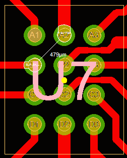
3. Check Pin Gap Rules - This function in Stencil Analysis checks whether the gaps between the pins of a component on the PCB are large enough to prevent short circuits during soldering. If the pin spacing is too small, there is a risk that the solder mask between the pins will break and solder paste will get under the components, which can lead to short circuits or other faults. Control testing can help to detect and correct such problems at an early stage to ensure optimum quality of PCB production.
The result is visible in the Pitch Rule Column, it shows the check value individualy for each component (ser via percent value).
Formula for Distance Percent is Pad Width (smaller side) * given Percent Value
4. Check Metal in Paste Volume Rules - This function checks the ratio between the metal volume and the paste volume (metal-in-paste volume ratio). Excessive metal deposition in the paste volume can impair soldering performance and lead to faults and defects.
5. There are also Option for the Squeegee. You have to mark the "Check Squeegee Direction Rules", it can handle two directions (horizontal and vertical). Depending on your squeegee type it has different distance rules.
6. Check drill in paste. For some drill types it is important to do not have them in the paste, maybe it run away throug the holes. You have only one parameter for an minimum drill diameter, to ignore very small drills.
7. Check MPN Pins. If you have a library connection to e.g. our EPL, you have real pin sizes and positions in the paste pads. With distance checks in all directions you make sure that the placed component is perfectly connected to the PCB.
8. Stencil Distances. Check the stencil opening distance for maximum values in the same network. It is possible for the paste to bond across the copper connection area, so it is recommended to check the distances in the same network.
Note: If you run the distance check and the pin gap rule it is filtered in both groups, we try to do not show double distance issues.
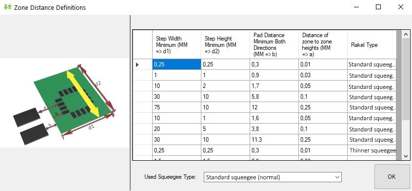
For Squeegee direction Rule it is possiblte to define many rules in the sub dialog:
This tool checks the orientation and direction of the squeegee used in the printing process of your circuit board. The tool ensures that the squeegee is aligned correctly to prevent issues such as smudging, misregistration, and insufficient solder paste deposition. The user can define the squeegee direction rules for each component on the board and the tool will check if they are being followed.

The results contain information such as the Area Ratio with an default Ratio = 2.000. To display only the requested results, it is possilble to filter each of the attributes (blue box) shown below using a term (red circle).

Stencil thickness indicates the thickness of the stencil. Since the wall surface of the solder pastes openings determines the thickness of the stencil, it must be selected as thin as necessary and as thick as possible. The thickness of the stencil is an important factor for its longevity, but it negatively affects the adhesion of the soldering paste.
Check only in PCB Profile allows the examination of PCBs across the PCB edge and enables to include the exterior.
In order to secure the results, you can find the option "export"/ "export to file" under the the tab "file" or in the lower right corner. It stores the results in a CSV file.
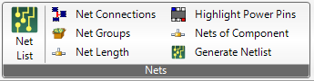
The NetGroup Wizard can be used to create net groups and to add or remove nets to them.
Open the NetGroup Wizard with clicking the "Net Groups" button.
The following dialog will show up.
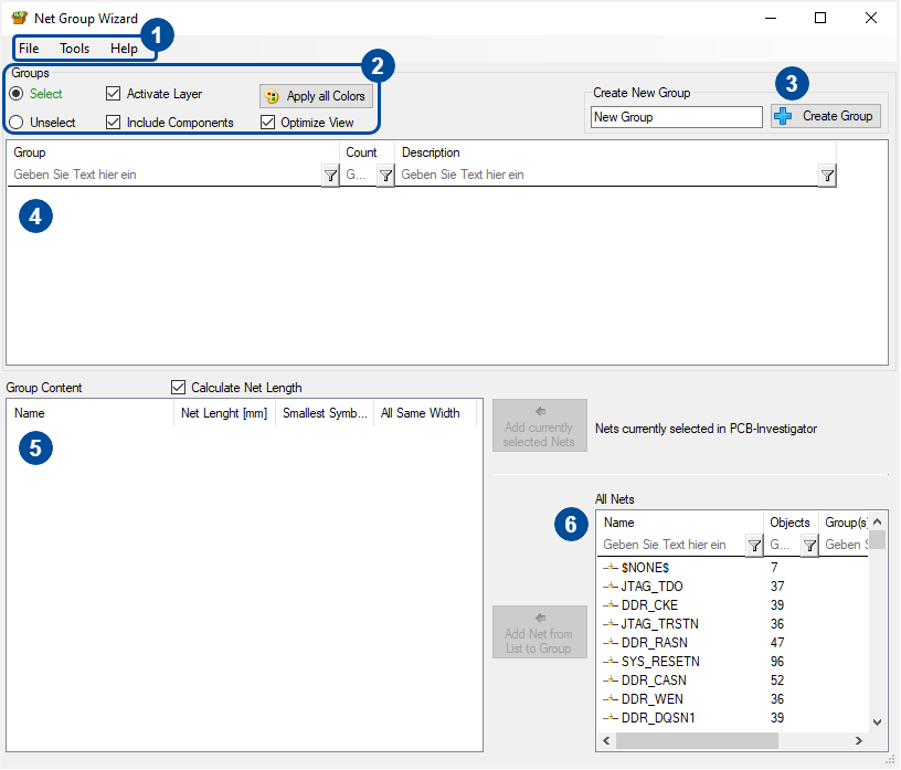
1. The two important tabs contain the following options.
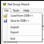
The net groups are always stored within the ODB design. Sometimes, you want to import net groups from another design. Prior to that, export the current net group to have a backup of them. In the import you can select between different file formats (xml, txt, dcf, dcfx, csv, rulf) to add net groups from other software (e.g. Xpedition or Zuken) or if you select xml from other PCB-Investigator exports.
Import Format List:
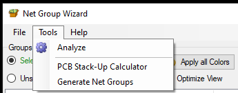
The "Tools" tab has three important functions.
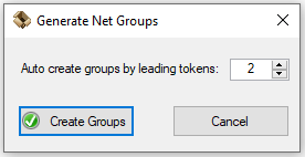
To create net groups, the net names will be used. The number is the number of letters to be tapped. All nets with the same beginning will then be added to the net group. The net groups names depend on the tapped letters.
2. The summary of controls allow you the following operations:
3. The button "Create Group" allows you to create you own groups with the desired group name.
4. This control contains all net groups which are deposited in the ODB dataset. More options to edit net groups can be found by right clicking on a net group.
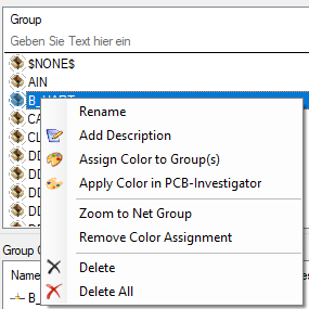
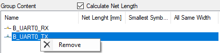
5. Every net of the net group will be shown here, if a group in the group view (4) is selected. To remove a net of the net group, right click the net you want to remove and click remove.
6. If y net group (4) is selected, you can add single nets to the net group with clicking a net in the view with the number 6 and clicking the add button. There are two different add buttons:
For more details have a look to this short video:
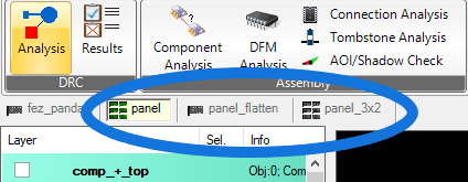
The plugin DFM Analysis can be found under the grid "Analysis" respectively "Assembly".
Here you will find six tab pages available for performing the DFM analysis: "Selective Soldering", "Fiducial Marker" (AOI verification), "Panelization" (technical verification of panels), "Testpoint", "Solder Paste" and "Trace Under Component". These single analysis functions are described below.
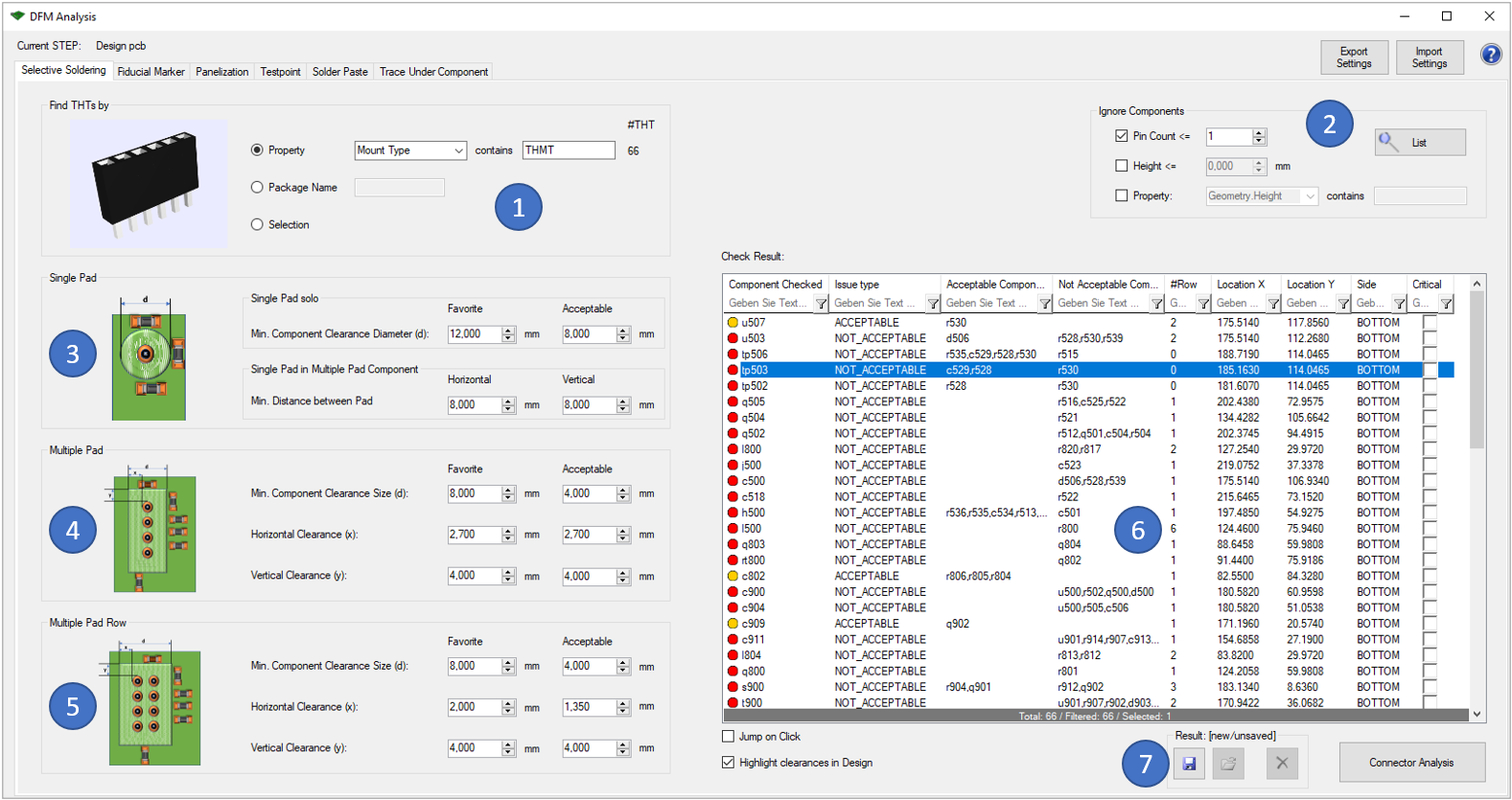
To begin with, the first topic is "Selective Soldering". This checks whether the set THT components will fit at the given location or whether the pins or holes of the THT component may be too close to components on the opposite side. The THT components you want to check can be selected either by the property or by the package name. It is also possible to directly select the THT components (1).
Before you can start the "Connector Analysis", you have to define the settings for the analysis. There is a distinction between "Single Pad" (3), "Multi Pad" (4) and "Multi Pad Row" (5). For each case, you can individually define the settings that will be used for the analysis. The pictures are intended to illustrate these variables. Each variable is determined by two different values, the "favorite" or optimum value and the "acceptable" value up to which manufacturability (according to your specifications) is still guaranteed.
The results of the analysis are then displayed in the table on the right-hand side of the window (6). Right-click to export them in HTML format. You can also use the tool to display the result. Components in the yellow area are located in the range you have defined as still acceptable. If a component is within the red area, the producibility with the current design is not guaranteed or the specifications defined by you are not fulfilled. Critical errors can also be marked for later use (e.g. in the 'Extended Design Report')
Following picture shows an example error of this analysis:
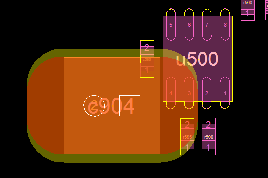
The THT component c904 is located on top side, but soldered on bottom side. The yellow marked components are too close to the soldered pins according to the 'Multi Pad' rule. The red area shows the "Acceptable" area, the yellow one is the "Favorite" area.
The following functionalities are equally integrated in all six options:
The "Fiducial Marker" analysis allows you to check whether the markers set for the AOI analysis can be implemented according to the selected specifications.

To do this, you must first search for the fiducials in your design (1). Four options, "Pad Usage", "Pad Geometry Name", "Package Name" and direct selection via the tool are provided for this purpose.
You can check the found fiducials for their manufacturability with 3 different parameters (3): "Copper Diameter", "SolderMask Diameter" and "Component Clearance Diameter". The check is then performed using these settings. Again, the results are displayed in the table on the right (4) or can be viewed directly via the tool. Critical errors can also be marked for later use (e.g. in the 'Extended Design Report').
The following functionalities are equally integrated in all six options:
The "Panelization" option allows you to check whether your panel meets the specified measurements. In order to be able to start the analysis for the "Panel Dimensions", you must first switch to "panel" in the tool.
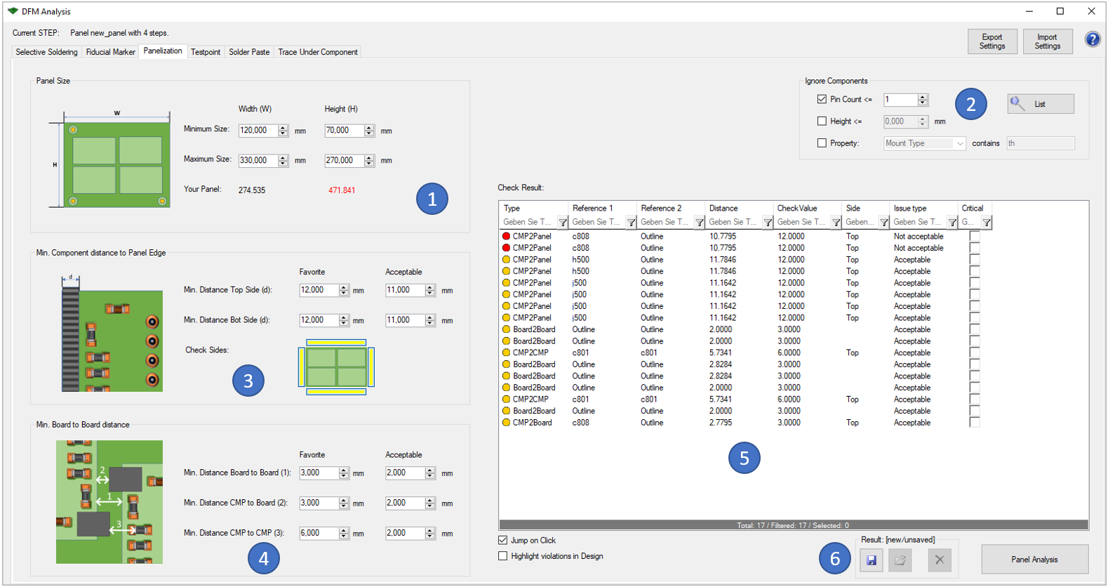
The size of the panel can be checked in the first block "Panel Size" (1).
You can also set the "Minimum Distance to Panel Edge" between components and the edge of the panel (3). At the same time, you have to choose an optimal value ("favorite") and a boundary value ("acceptable"). If the acceptable value is not reached, the producibility of the panel is endangered. Furthermore, you can decide, which edge of the board should be checked ("check sides").
Last you can analyze the "Board to Board distance" (4). Here the distance between boards, as well as the distance between component and foreign board, and component to component can be checked. Again you can enter an "Acceptable" and "Favorite" distance.
The results of the analysis are displayed in the window on the right (5). You can also view the analysis results directly in the tool. Critical errors can also be marked for later use (e.g. in the 'Extended Design Report').
Following picture shows an example error of this analysis:
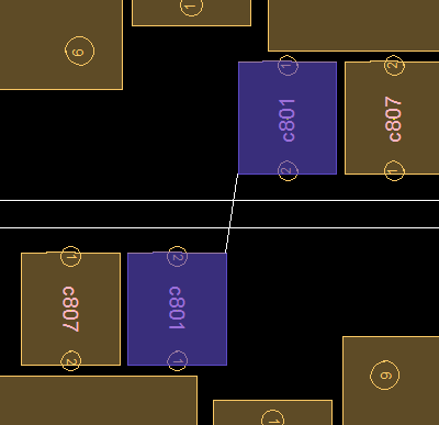
The component c801 of one board is too close to the same component on the neighbored board.
The following functionalities are equally integrated in all six options:
The "Testpoint" option allows you to check the distance between testpoints and between testpoint and components. This analysis is important to ensure e.g. the manufacturability of ICT adapters.
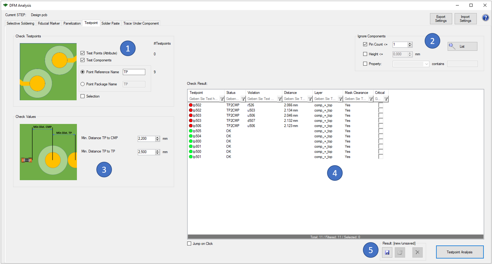
In the first block (1) there are different options to identify test points:
With the block "Check Values" (3), you can enter the wanted distances between testpoints (center to center) or between testpoint and components (center to outline).
The results of the analysis are displayed in the window on the right (4). You can also view the analysis results directly in the tool. Critical errors can also be marked for later use (e.g. in the 'Extended Design Report').
Following picture shows an example error of this analysis:
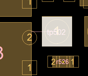
A component is too close to the test point tp502.
The following functionalities are equally integrated in all six options:
The "Solder Paste" option allows you to check if all component pins have a solder paste object, a copper pad, and a solder mask clearance defined and if the solder paste is inside a solder mask clearance.
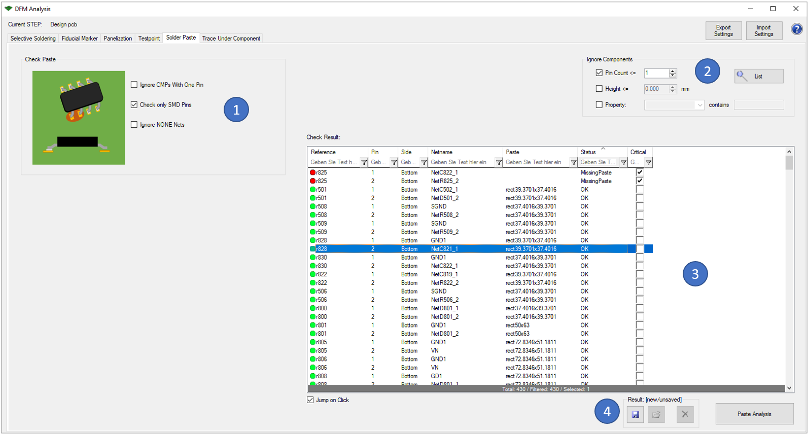
In the first block (1) you can define which components should be analysed. Here you have following ignore options:
The results of the analysis are displayed in the window on the right (3). You can also view the analysis results directly in the tool. Critical errors can also be marked for later use (e.g. in the 'Extended Design Report').
Following error types are reported:
The following functionalities are equally integrated in all six options:
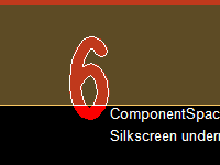
The "Trace Under Component" option allows you to check, if certain components have unallowed copper tracks under their body between their pins. This is mostly unwanted for small 2-pin components, as it can cause problems during soldering.
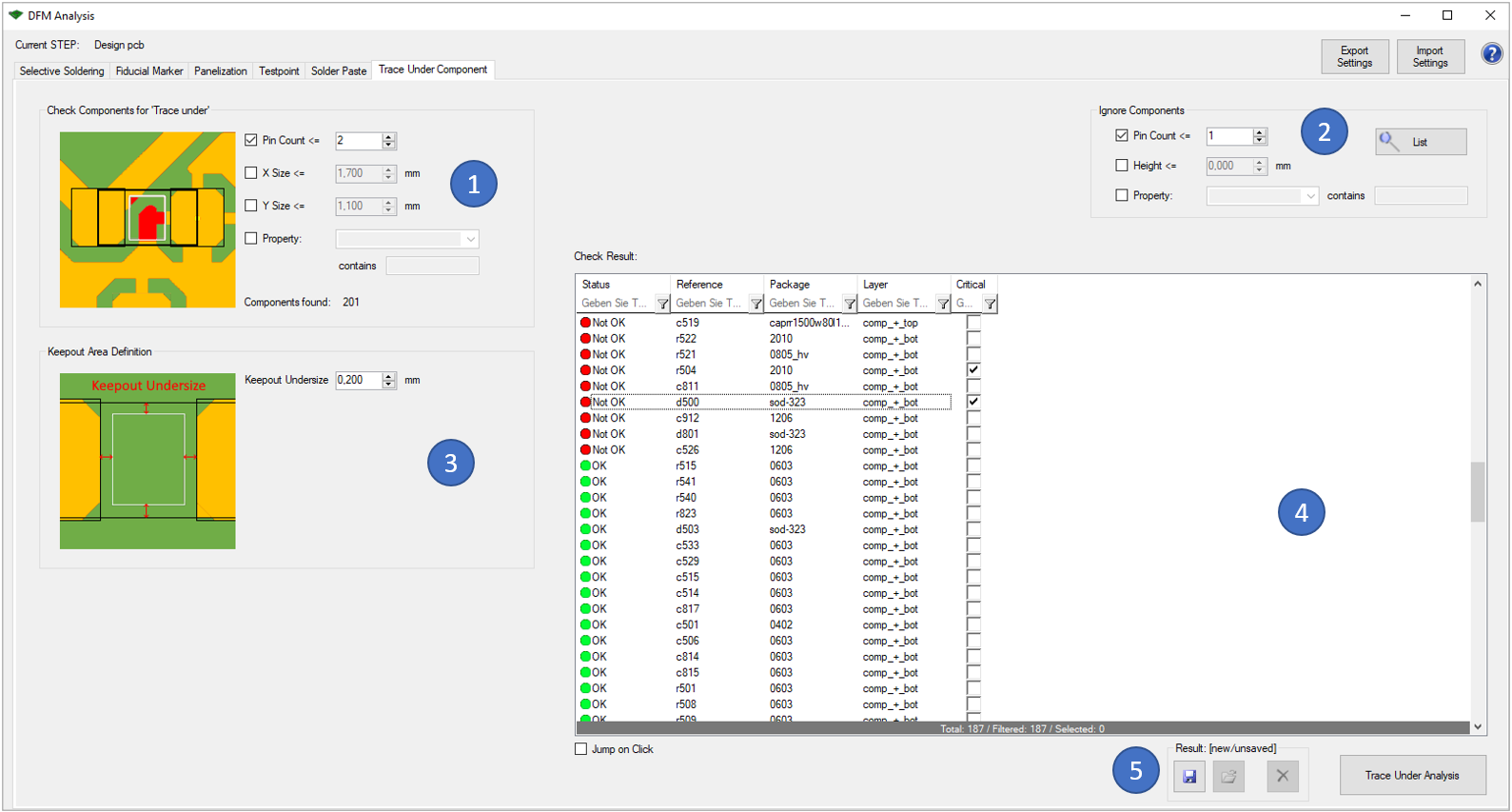
In the first block (1) there are different options to identify the components that should be analyzed:
With the block "Keepout Area Definition" (3), you can enter the wanted undersize that is used to determine the keepout area under the component body and between its pins.
The results of the analysis are displayed in the window on the right (4). You can also view the analysis results directly in the tool. Critical errors can also be marked for later use (e.g. in the 'Extended Design Report').
Following picture shows an example error of this analysis:
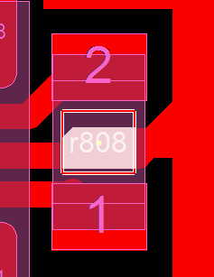
The component "r808" has unwanted copper tracks under its body inside the keepout area.
The following functionalities are equally integrated in all six options:
The plugin Component Analysis can be found under the grid "Analysis" respectively "Assembly".
Here you will find two tab pages available for performing the Component Analysis: "Component Distance Analysis" and "Component Placement Analysis". These single analysis functions are described below.
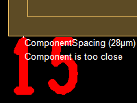
The "Component Distance Analysis" option allows you to check the distance between components and between components and the board outline. This analysis is important to ensure e.g. the manufacturability during the placement and soldering process.
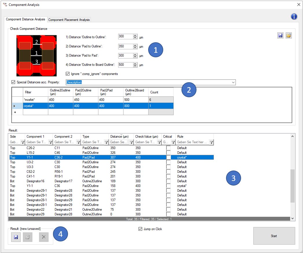
In the first block (1) you can define the different check values:
Here you also have the possibility, to ignore unplaced components (by ignoring components with a ".comp_ignore' attribute).
In the second block (2), you can define "Special Distances acc. Property". That means, you can define the same set of rules as in (1) but with different values for sub groups of components. The Filter is matching a literal string, but wildcards like " * " can be used to make more broad filter settings e.g. 0602*. The sub groups are build by a given component property. Examples are:
The results of the analysis are displayed in the window on the bottom (3). You can also view the analysis results directly in the tool. Critical errors can also be marked for later use (e.g. in the 'Extended Design Report').
With the buttons on the top right side of the window you can export the previously defined settings so that you can reuse them for later analyses. Already saved settings can be imported via the "Import Settings" button.
The last result can be saved and reloaded with the buttons on the lower left side (4). This stored result is also used in the 'Extended Design Report'.
Clicking on the question mark on the top right of the window opens the corresponding page of our online manual.
Following picture shows an example error of this analysis:
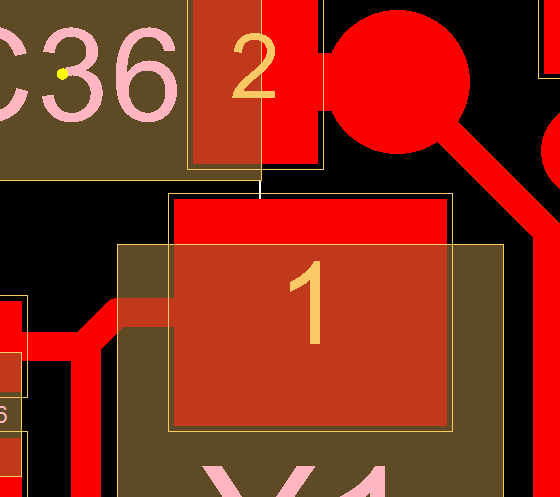
The copper pad of the X1-1 is too close the the component body of C36.
The "Component Placement Analysis" option allows you to check, if the MPN Package of a component fits the CAD Package.
A MPN Package (MPN = Material Part Number) is the real component outline of a part. This outline is often much smaller than the corresponding CAD package body. The MPN Package can also contain the contact surface of the pin. In this analysis, this contact surface of the pins is analyzed. You can define, where the contact surface has to be situated inside the copper pad.
A standard design has no MPN Package definitions included. EasyLogix offers the 'EasyLogix Part Library' (EPL) to add detailed part information like datasheets, MPN packages, 3D step files, ... to your design.
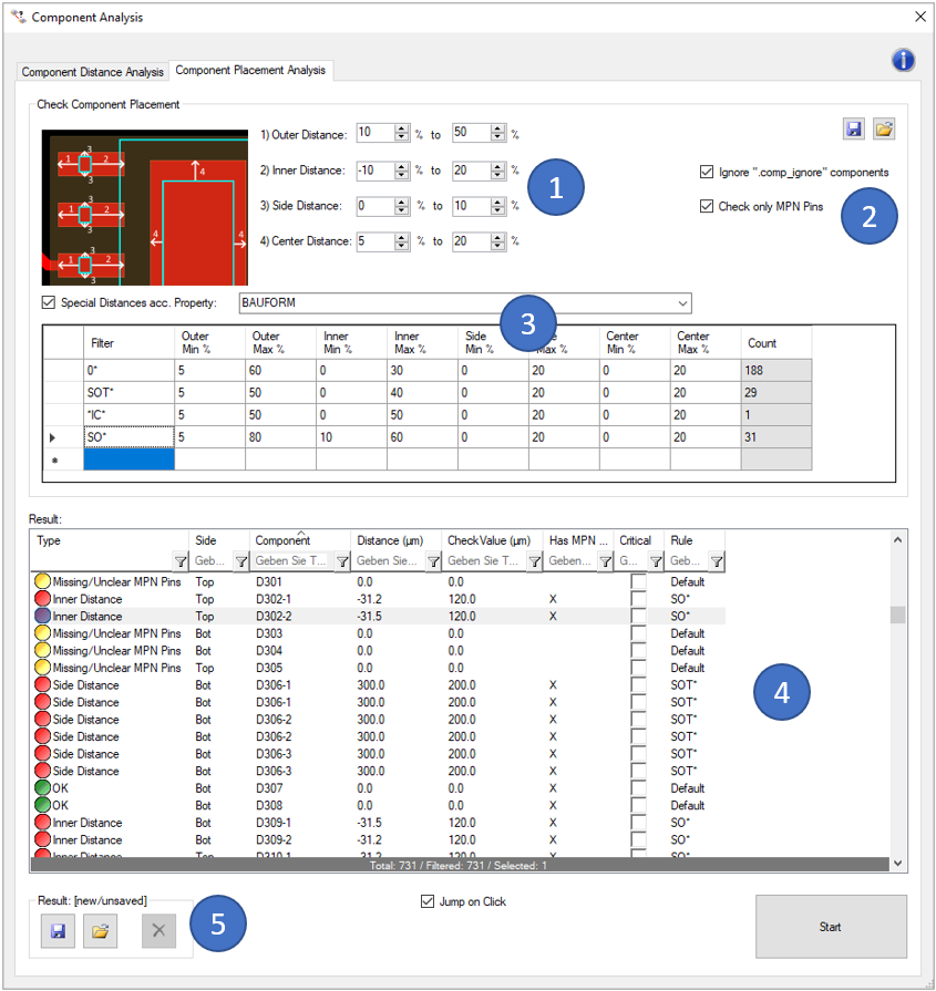
In the first block (1), you can define the different check values:
In the second block (2), you can define filters to ignore unplaced components (by ignoring components with a ".comp_ignore' attribute) and components without MPN package definitions.
In the third block (3), you can define "Special Distances acc. Property". That means, you can define the same set of rules as in (1) but with different values for sub groups of components. The Filter is matching a literal string, but wildcards like " * " can be used to make more broad filter settings e.g. 0602*. The sub groups are build by a given component property. Examples are:
The results of the analysis are displayed in the window on the bottom (4). You can also view the analysis results directly in the tool. Critical errors can also be marked for later use (e.g. in the 'Extended Design Report').
With the buttons on the top right side of the window you can export the previously defined settings so that you can reuse them for later analyses. Already saved settings can be imported via the "Import Settings" button.
The last result can be saved and reloaded with the buttons on the lower left side (5). This stored result is also used in the 'Extended Design Report'.
Clicking on the question mark on the top right of the window opens the corresponding page of our online manual.
Following picture shows an example error of this analysis:
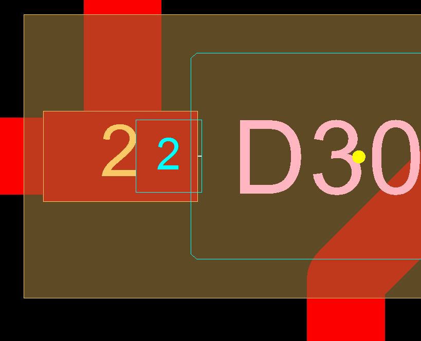
The contact surface of the pin 2 of the MPN Package for D30 is not matching the "inner distance" rule. That means in this case, the pin's contact surface is partly outside the copper pad. A reason could be, that the choosen part (MPN) does not fit to the CAD data. Soldering issues and failures are likely.
All Plugins have the following two Interfaces for direct calls from the outside.
///<summary
/// Analysis interface for scripts and plugins.
///</summary
→ The Header from the first Interface.
public interface IPCBIAnalysis {
///<summary
/// The name of this analysis to identify it with the settings.
///</summary
string Name { get; }
///<summary
/// The readable name of this analysis
///</summary
string Title { get; }
///<summary
/// The path to the results directory of this analysis relative to the job path
///</summary
string ResultsFolderName { get; }
///<summary
/// The preview icon for this analysis
///</summary
Icon PreviewIcon { get; }
///<summary
/// Set if the file preview should show if results are available
///</summary
Set if the file preview should show if results are available
///<summary
/// Create a instance of rules to define the default standard rules.
///</summary
PCBI.Automation.Rules.RulesContainer GetStandardRules();
// void AddToUpdateProgress(PCB_Investigator.PCBIWindows.PCBIWorkingDialog working, int minValue, int maxValue);
// bool Execute(string ResultFilePath);
public interface IPluginAnalysis: IPlugin, IPCBIAnalysis{
///<summary
///
///</summary
///
void AddToUpdateProgress(PCB_Investigator.PCBIWindows.PCBIWorkingDialog working, int minValue, int maxValue);
bool Execute(IAnalysisParams analysisParams);
bool Execute(string resultFilePath); }
→
The script is allowed to increment
values between minValue and maxValue.
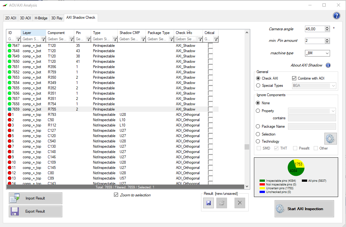
For all AXI machines you can perform the shadow check. This test checks if the material is covered from bottom to top and inverted.
It also supports combination with AOI machines, you have settings for each package type to set the check, e.g. for a chip component it should check only with orthogonal AOI camera, for qfn components with angle camera and for bga all pins checked with AXI analysis.
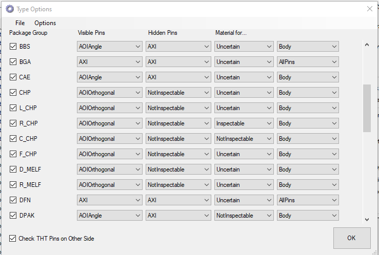
For each package group you can define the visible pins, hidden pins and material for body and or pins:
Machine Definition
Each machine has many options to define the cameras, the check methods (AXI, AOI Angle, AOI Orthogonal) with camera angle and the list for all package groups.
If you do not use package groups it use for all the Default rule, this means the visible pins checked by AOI Angle cameras and the hidden pins checked by AXI.
You can handle a list of different machines and use the quick selection in the main dialog to run your analysis directly.
Filter
For all AOI/AXI Analysis checks you can filter for different options like technology (SMD, THT, Pressfit, Other) and properties e.gl Comp Ignore and/or No Pop attribute.
There is also a variant handling option to filter the variant by name.