The plugin Component Analysis can be found under the grid "Analysis" respectively "Assembly".
Here you will find two tab pages available for performing the Component Analysis: "Component Distance Analysis" and "Component Placement Analysis". These single analysis functions are described below.
The "Component Distance Analysis" option allows you to check the distance between components and between components and the board outline. This analysis is important to ensure e.g. the manufacturability during the placement and soldering process.
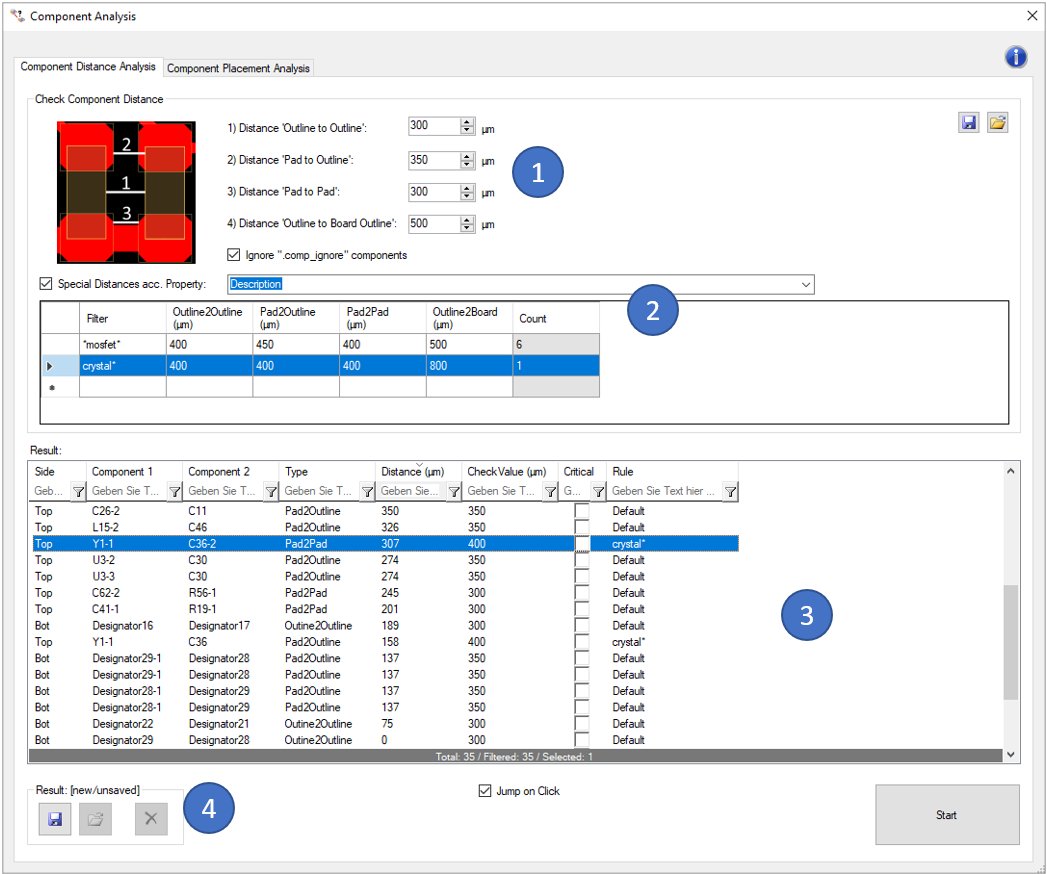
In the first block (1) you can define the different check values:
Here you also have the possibility, to ignore unplaced components (by ignoring components with a ".comp_ignore' attribute).
In the second block (2), you can define "Special Distances acc. Property". That means, you can define the same set of rules as in (1) but with different values for sub groups of components. The Filter is matching a literal string, but wildcards like " * " can be used to make more broad filter settings e.g. 0602*. The sub groups are build by a given component property. Examples are:
The results of the analysis are displayed in the window on the bottom (3). You can also view the analysis results directly in the tool. Critical errors can also be marked for later use (e.g. in the 'Extended Design Report').
With the buttons on the top right side of the window you can export the previously defined settings so that you can reuse them for later analyses. Already saved settings can be imported via the "Import Settings" button.
The last result can be saved and reloaded with the buttons on the lower left side (4). This stored result is also used in the 'Extended Design Report'.
Clicking on the question mark on the top right of the window opens the corresponding page of our online manual.
Following picture shows an example error of this analysis:
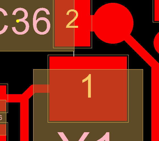
The copper pad of the X1-1 is too close the the component body of C36.
The "Component Placement Analysis" option allows you to check, if the MPN Package of a component fits the CAD Package.
A MPN Package (MPN = Material Part Number) is the real component outline of a part. This outline is often much smaller than the corresponding CAD package body. The MPN Package can also contain the contact surface of the pin. In this analysis, this contact surface of the pins is analyzed. You can define, where the contact surface has to be situated inside the copper pad.
A standard design has no MPN Package definitions included. EasyLogix offers the 'EasyLogix Part Library' (EPL) to add detailed part information like datasheets, MPN packages, 3D step files, ... to your design.
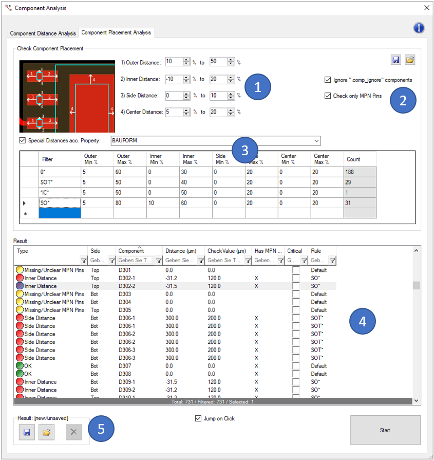
In the first block (1), you can define the different check values:
In the second block (2), you can define filters to ignore unplaced components (by ignoring components with a ".comp_ignore' attribute) and components without MPN package definitions.
In the third block (3), you can define "Special Distances acc. Property". That means, you can define the same set of rules as in (1) but with different values for sub groups of components. The Filter is matching a literal string, but wildcards like " * " can be used to make more broad filter settings e.g. 0602*. The sub groups are build by a given component property. Examples are:
The results of the analysis are displayed in the window on the bottom (4). You can also view the analysis results directly in the tool. Critical errors can also be marked for later use (e.g. in the 'Extended Design Report').
With the buttons on the top right side of the window you can export the previously defined settings so that you can reuse them for later analyses. Already saved settings can be imported via the "Import Settings" button.
The last result can be saved and reloaded with the buttons on the lower left side (5). This stored result is also used in the 'Extended Design Report'.
Clicking on the question mark on the top right of the window opens the corresponding page of our online manual.
Following picture shows an example error of this analysis:
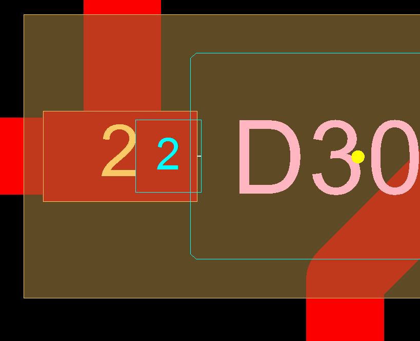
The contact surface of the pin 2 of the MPN Package for D30 is not matching the "inner distance" rule. That means in this case, the pin's contact surface is partly outside the copper pad. A reason could be, that the choosen part (MPN) does not fit to the CAD data. Soldering issues and failures are likely.
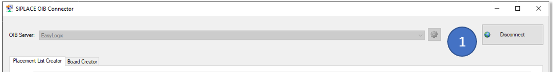
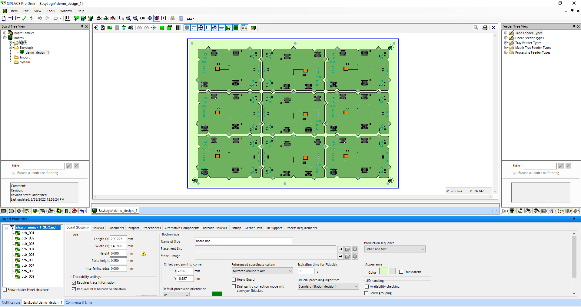
When you open the "SIPLACE OIB Connector" (in the 'Machine Export' menu) the first time, you have to first enter your OIB server settings by clicking on the gear button (1):
Following dialog will open:
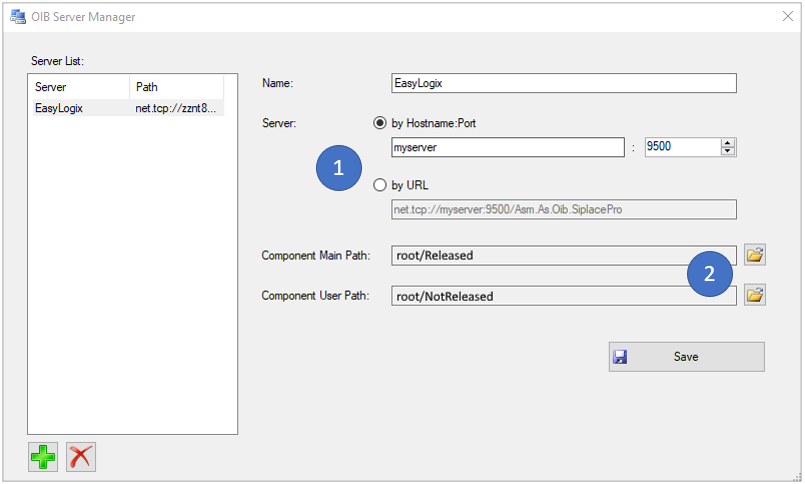
In this server manager, you can organize multiple OIB servers. To create a new one, please press on the little green "+" button and enter a name.
Afterwards you'll have to specify the OIB server adress by entering an IP/Hostname + Port, or directly enter the 'net.tcp://...' adress (1).
When this is done, you'll have to specify two server directories by clicking on the small browse button (2):
Click "Save" and close the dialog to preceeed.
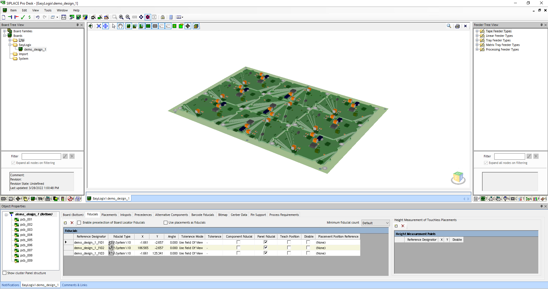
To start, please select a server and click "Connect" (1).
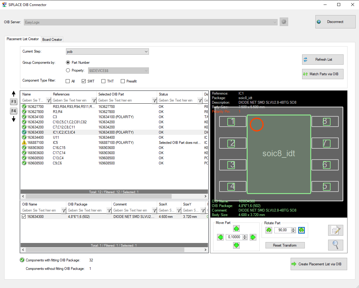
With the "Placement List Creator" tab, you can create placement list elements for each component side on the OIB server.
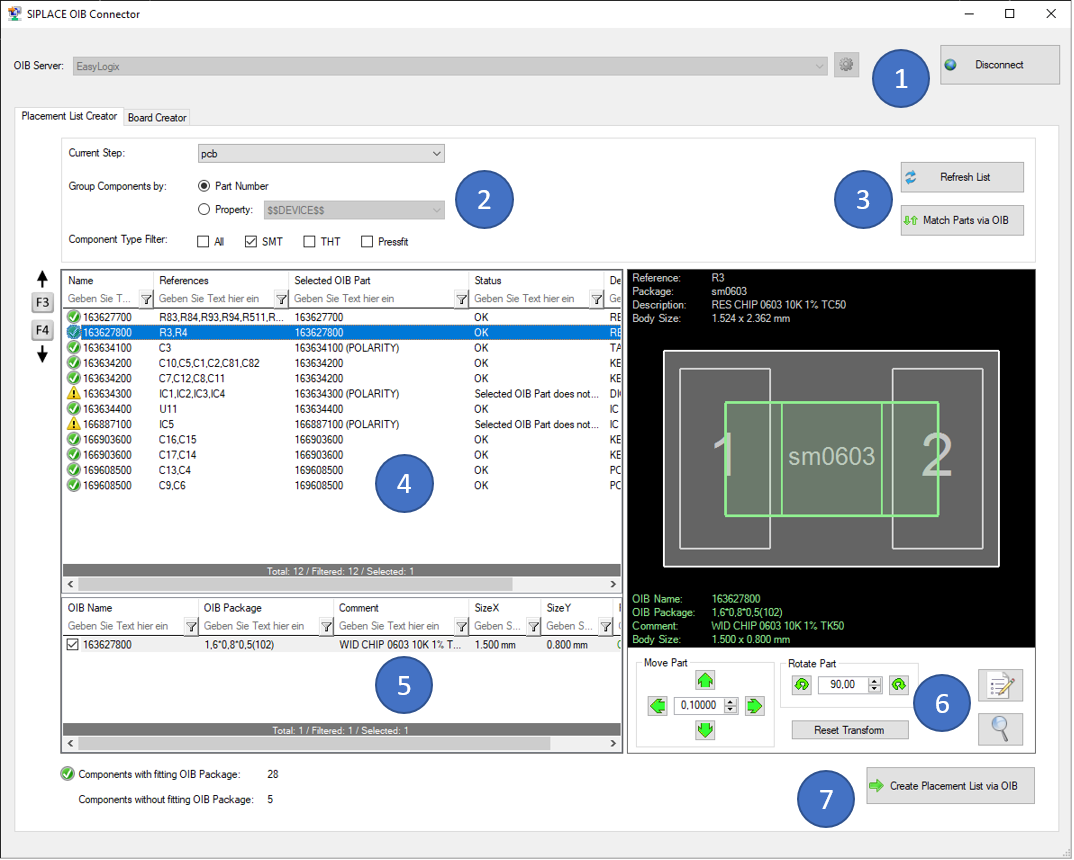
To start, you have to do a few settings in block (2):
Always when you change settings in (2), you will have to 'Refresh' the list and 'Match Parts via OIB' again (3).
When the matching process is done, you will see all your filtered parts in the list (4), including an overlay of the matching OIB part definition on the selected server. Found OIB parts are centered on the CAD package center. Details of the found OIB part and the fitting state are listed on the bottom side (5).
The 'Status' column indicates, whether a OIB part was found or not, and if the found part fits onto the CAD package. The condition for fitting is, that the pin definition of the OIB part must at least partly overlap the CAD package pin.
If the found part does not fit, you have the possibility to shift its position or to rotate it until it fits (6). With the two buttons in this block on the right, you can open the property dialog of the CAD component or zoom to it.
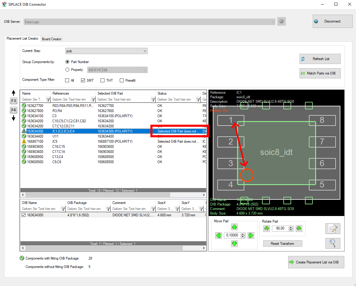
If the OIB part has a polarity definition, this polarity marker is visualized in red. The fitting alorithm then also uses the polarity information, to recognize if the component is correctly rotated (CAD polarity pin is same as OIB polarity pin).
Example of the fitting process (6) (by rotating 90° clockwise):
 =>
=> 
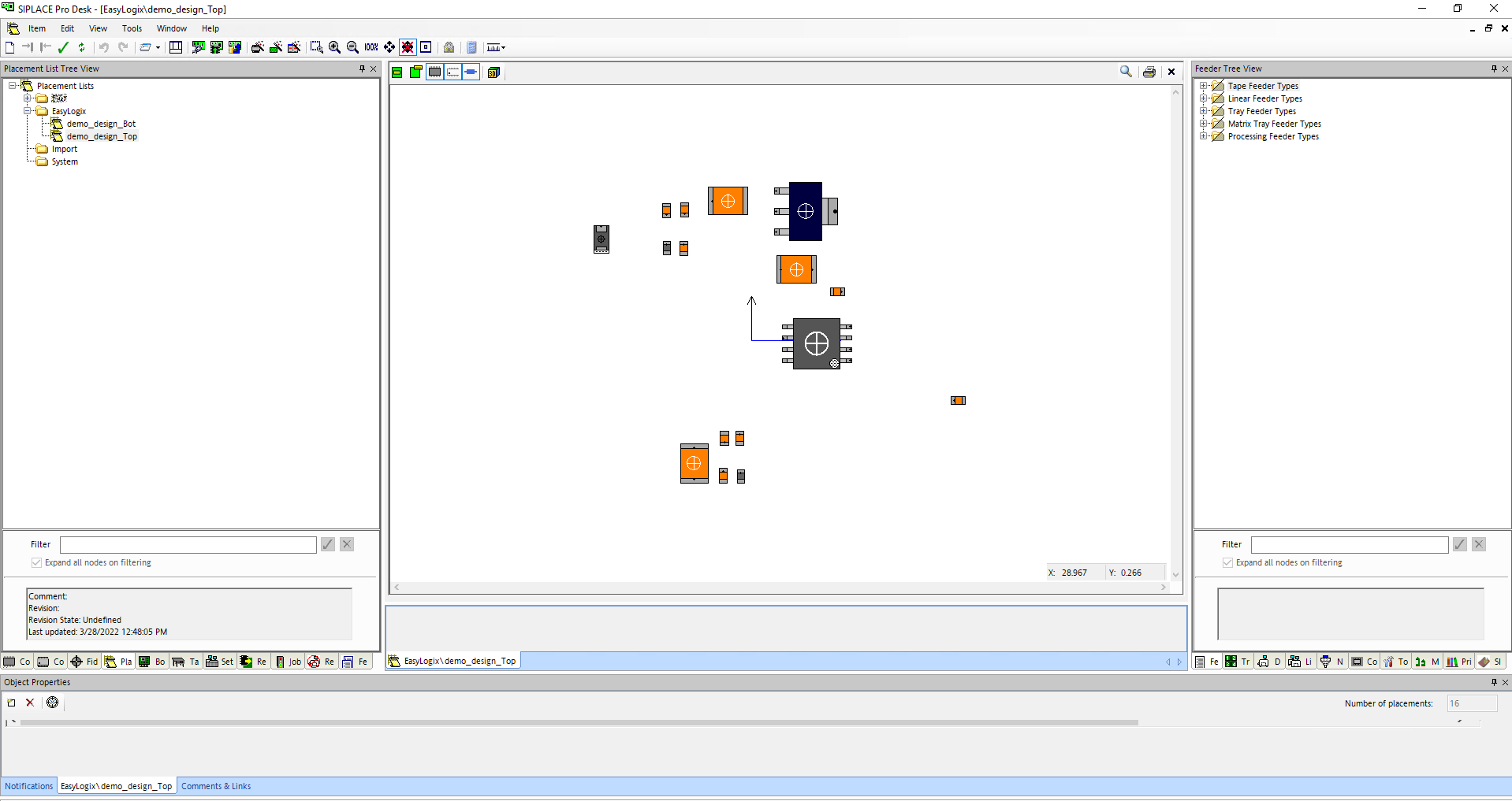
When clicking the 'Create Placement List via OIB' button (7), you are asked to select a folder on the OIB server and enter the name for the placement list(s) for top and/or bottom side. Afterwards, the placement lists are created via OIB. Missing parts, that where not found during the matching process, are automatically created in the 'Component User Path' (see 'OIB Server Manager'). Those created parts are dummy parts without any real outlines or pin definitions. Their information must be completed by the user in the SIPLACE Software afterwards. Components that have the ".comp_ignore" attribute are marked as 'omitted' in the placement list.
Here is a screenshot of the result in the SIPLACE Software:
After having created the placement list of the single board(s), you can create the panel data with the "Board Creator" tab.
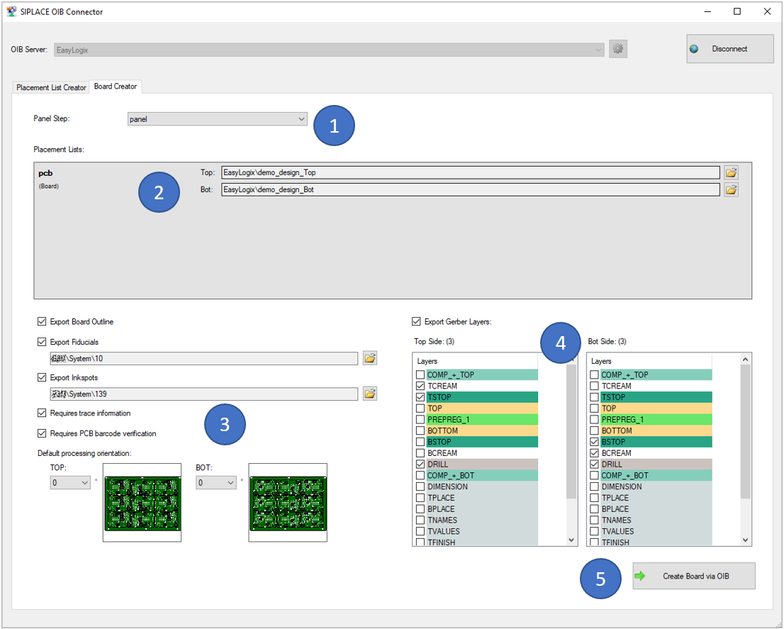
To start, you have to select the panel step that should be created (1). It is also possible to create panels in panels (recursive), when the most outer panel is selected.
For the given panel, the included single board(s) is/are listed unter (2). Here an already existing placement list on the OIB server must be selected per board and side. If the placement lists where created before in this session with the "Placement List Creator", the information is already prefilled. If not, you can click the small browse button and select the right placement list.
In the block (3), there are different options available:
In the block (4), you can choose which CAD layers should be exported and imported in OIB for this board per side. It is mainly thought for paste/mask layers.
When clicking the 'Create Board via OIB' button (5), you are asked to select a folder on the OIB server and enter the name for the board entry. Afterwards, the board is created via OIB.
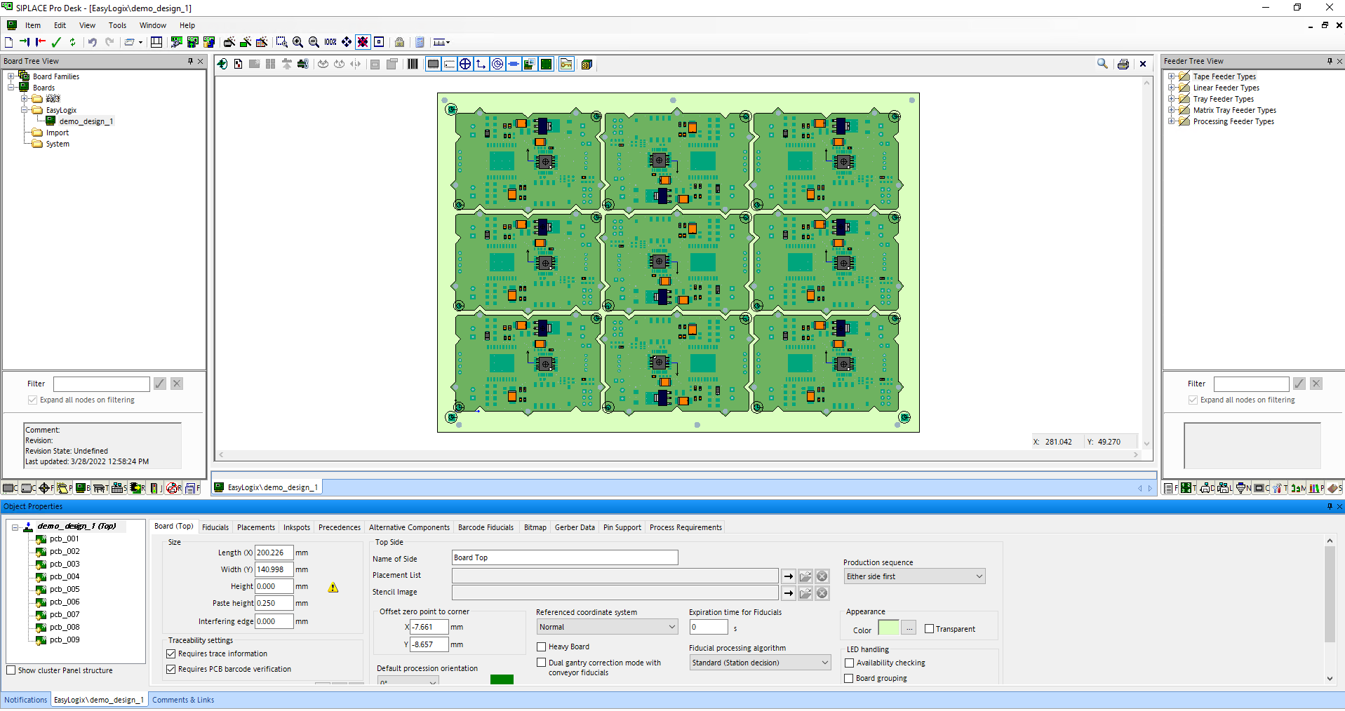
Here is a screenshot of the result in the SIPLACE Software:
With the "SIPLACE QD Exporter" tool, you can create '.qd' files including placement lists and board information for ASM machines.
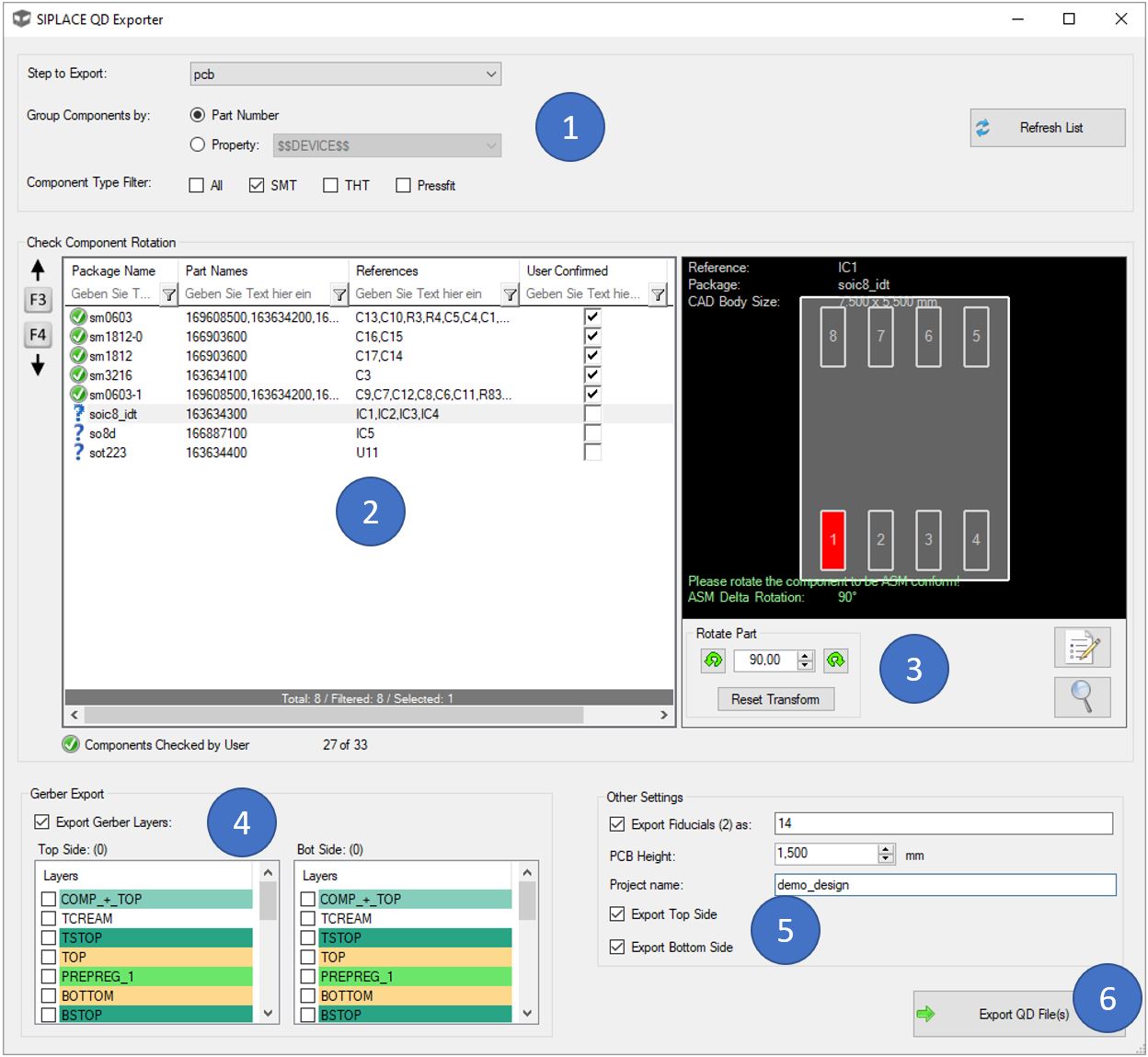
To start, you have to do a few settings in block (1):
Always when you change settings in (1), you will have to click at 'Refresh' to update the list. In the list (2), you will see all packages and the corresponding parts for each step or sub-step of your selected (panel) step.
It is then important so select list entry by list entry to check the rotation correction. If a entry is selected, you'll see the package drawing on the right side. You have to rotate this package to be displayed in exactly the same way, as it is defined on the ASM machine ('make it ASM conform'). You can confirm this by checking the "User Confirmed" checkbox in the list's last column. The rotation can be done by using the buttons in (3). Here, the rotation can also be reset and with the two buttons in this block on the right, you can open the property dialog of the CAD component or zoom to it.
In the block (4), you can choose which CAD layers should be exported as gerber files next to the '.qd' file. These gerbers can then be also imported in SIPLACE. The mirroring/translation of the bottom gerber is already done in the gerber itself, so that you do not need to transform the layers in SIPLACE.
In the block (5), there are different options available:
When clicking the 'Export QD File(s)' button (6), you are asked to select a folder where the files are exported to.
Here are some screenshots of the result in the SIPLACE Software:
The Component Report in PCB-Investigator is a useful tool to get a summary of all components used in the PCB. This can be very helpful to make sure that all required components are present on the board and to make sure that they are placed and wired correctly.
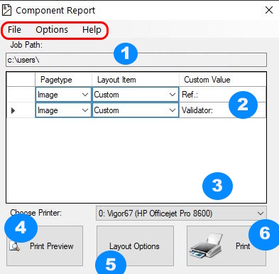
1. The path of the currently loaded job is displayed here
2. The window is for customizing temporary field contents of the layout.
All items of the layout type "Custom" are listed here. The changes are
only temporary.
3. With this button you can choose your printer
4. With this button you can see the print preview
5. At "Layout Options" you can set the options for creating the layout.
More about this in the following paragraph.
6. The Last Button is for printing your Component Report
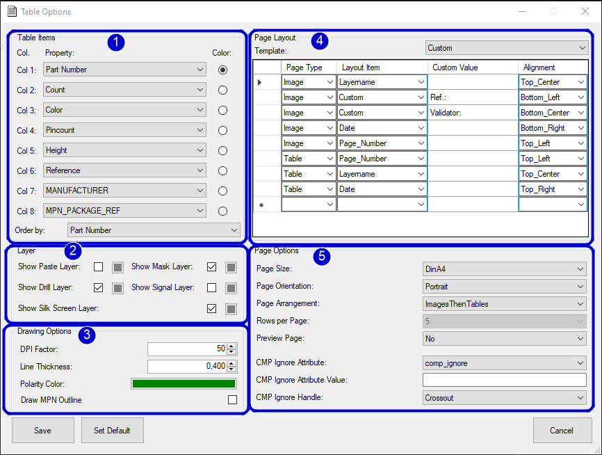
1. Tablepartitioning sets which attributes/properties of the CMP should be listed and which attribute/property should be used for coloring (Component with same attribute value get same color)
2. Layer options gives you the possibility to display different layers during printing
3. Drawing Options can be used to change the color or thickness if you like
4. Layout of the side is used to create your own page layout and can be extended as you wish.
Pagetype: Image or TableCustom Value: Will only be filled if the item was set to Custom before. Values filled here will be saved in the layout.
Alignment: Used to determine where on the page this element should be placed. Same alignments lead to the fact that these are arranged afterwards under each other.5. Page Options gives you the options in which paper format to print. In addition, you can select how many lines of the table should be displayed on one page (0 means that the table will have its own page). Furthermore you can sort the table by attributes and choose between predefined page layouts like:
all three layouttypes are shown in the print preview at the end of this page.
Page Arrangement is Important only for Rows per page = 0 (table on extra page)
It is possible to ignore components with different options to hide them or crossout them.
All Plugins have the following two Interfaces for direct calls from the outside.
///<summary
/// Analysis interface for scripts and plugins.
///</summary
→ The Header from the first Interface.
public interface IPCBIAnalysis {
///<summary
/// The name of this analysis to identify it with the settings.
///</summary
string Name { get; }
///<summary
/// The readable name of this analysis
///</summary
string Title { get; }
///<summary
/// The path to the results directory of this analysis relative to the job path
///</summary
string ResultsFolderName { get; }
///<summary
/// The preview icon for this analysis
///</summary
Icon PreviewIcon { get; }
///<summary
/// Set if the file preview should show if results are available
///</summary
Set if the file preview should show if results are available
///<summary
/// Create a instance of rules to define the default standard rules.
///</summary
PCBI.Automation.Rules.RulesContainer GetStandardRules();
// void AddToUpdateProgress(PCB_Investigator.PCBIWindows.PCBIWorkingDialog working, int minValue, int maxValue);
// bool Execute(string ResultFilePath);
public interface IPluginAnalysis: IPlugin, IPCBIAnalysis{
///<summary
///
///</summary
///
void AddToUpdateProgress(PCB_Investigator.PCBIWindows.PCBIWorkingDialog working, int minValue, int maxValue);
bool Execute(IAnalysisParams analysisParams);
bool Execute(string resultFilePath); }
→
The script is allowed to increment
values between minValue and maxValue.
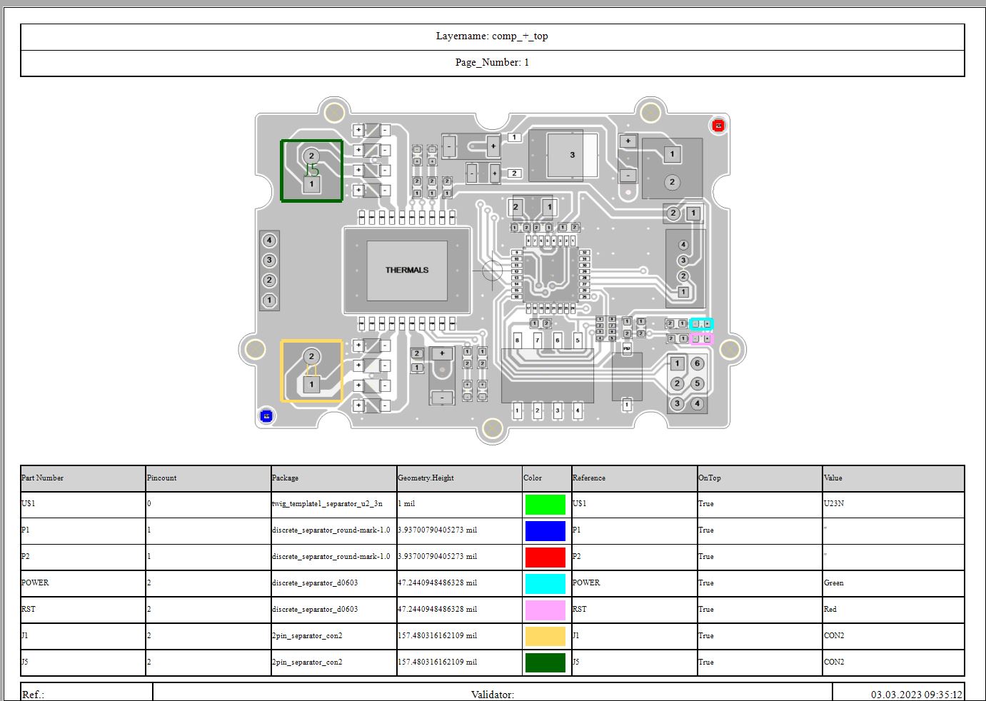
Custom Layout
HeaderFooter Layout
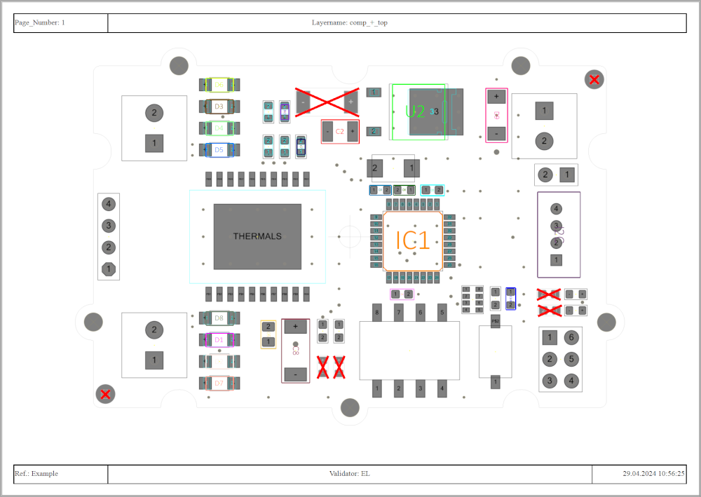
Crossout of Ignore Components
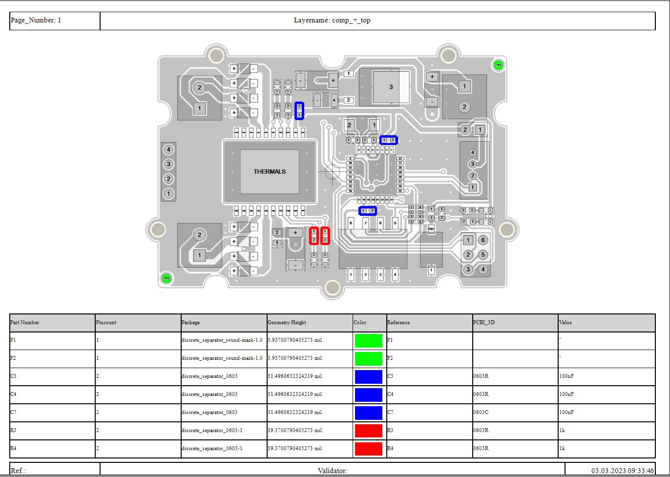
TopLeft Layout
You can configure the view that you see on the right (2) by selecting the wanted attributes and properties on the left side (1).
The Left Side is called the Property List while the right side is called the Component List
The properties selected on the left side will then show up on the right side. The order of the columns is determined by the order in which you have selected the properties in the listview on the right. If you want to change the order you can also drag and drop the different columns to the position you want. Important to note is that columns like id, reference and the SumUp Column will be moved back to the front after you reopen the Component Manager. Sum Up will add the different rows together and aggregate the rows based on the selected values.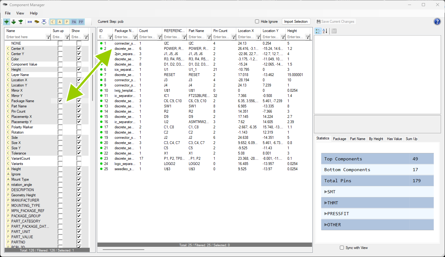
The different icons inside of the Property List define what kind of attribute it is, while the dot besides the component in the Component List shows the change status of the component. The legend for the different icons is as follows.

You can select multiple different settings to adjust the view quickly.
![]()
From left to right they to the following.
By right clicking the component list you can export the current view to and Excel or HTML file.

Items selected inside of the Component List can be edited inside of the property grid on the right side.

Any changes to the component will lead to the green dot turning orange. You can save the changes by either clicking the button above the property grid and saving or pressing the save option in "File" in the top row. Until then there are no changes that are actually saved and applied to the real components. If you select multiple components at the same time, or use the Sum Up which leads to a row representing more than one component, the property grid will show you only the values that are the same between all components. Any changes inside of the property grid will then edit all objects at the same time. Properties shown are not necessarly present in all components selected. If one component has the property then the property will be shown. If a value is then edited, the components that do not have the property will be given the property.
There are multiple statistics about the design that can be easily viewed in the lower right hand corner.
In total there are 6 different statistics that can easily be accessed inside of the different tabs.
The first tab shows the amount of top and bottom components that populate the board as well as the amount of pins on the board. Furthermore you can see the statistics also divided depending on the mounting type of the component.

The next tab shows the different packages that are used and how often they are used. Starting from this statistic you can choose between a bar chart or a pie chart with the radio buttons below the chart.


The next tab does the exact same just sorted by the Part Name instead of the Package.
The height tab looks at the different Heihgts that are present in the design and displays them.
The tab called "Has Value" inspects how many components have a certain property. You are able to select the different properties and find out if for example all components have a "MPN" property.
The Sum up Tab does the exact same as the sum up function inside of the Property List, but in the form of a bar or pie chart.
Connect Library information with your AVL File, with individual importer it can read csv, excel and other files.
Check all components with vidual fitting helper and maybe transform wrong locations or rotations with the simple user interface:

Depending on the MPN and Manufacturer the BOM Expert search for library information and connect them with the open design, this can include properties and step files. You can automatically set no_pop/comp_ignore attributes and use custom actions with an post script to do special actions depending on the imported data.
The Settings containing a list of importers, Searchend Properties and settings to handle not found components. It also has options to add missing entries in an intermediate library and an post script (found by GUID in your favorites).

Unknown => It is not possible to give more details
ReferenceNotInDesign => The reference in imported data is not available in the design
ReferenceNotInAVL => The component in the design has no entry in imported file
NoPartAvailable => The part list do not contain results in the selected library
NoPartSelected => No part selected mean the user has to select one
NotFoundInLib => The library do not contain a fitting item
SelectedPartDoesNotMatch => There is a maybe wrong part selected, please check the selected part
OK => Part is OK
OKUnverified => The pin matiching is not checked but the part is marked as OK
Essemtec Pick & Place Exporter
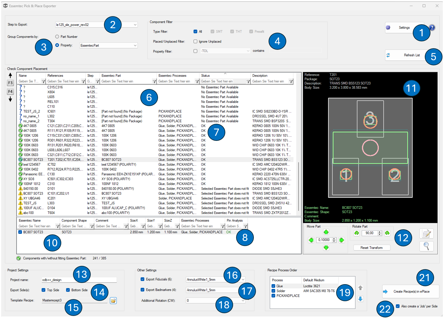
The Essemtec Pick & Place Exporter is used to create ePlace recipes from an ODB++ design loaded in PCB-Investigator. The dialog compares the CAD components from the selected ODB++ step with the Essemtec/ePlace component library, allows the user to check and correct package alignment, and finally creates the required recipe structure in ePlace.
The typical workflow is shown by the numbered areas in the dialog. Work through the dialog from top to bottom and from left to right.
Open Settings
Before the exporter can communicate with ePlace, the connection to the PCBIEssemtecServer must be configured. Press Settings to open the settings dialog.

Configure the PCBIEssemtecServer connection
In the settings dialog, select whether the server is used as a Local Server or a Remote Server. For a local server, enter the path to the installed PCBIEssemtecServer in Server Path. The server address is typically localhost. The Server Port defines the REST port used by PCB-Investigator.
The PCBIEssemtecServer is installed separately if required (contact support@easylogix.de to get the installation package). It provides a REST server for PCB-Investigator on one side and connects to the ePlace DLLs on the other side. PCB-Investigator communicates only with this server. The server performs the required ePlace library queries and creates the requested ePlace objects.
Press Save to store the settings. The exporter uses these settings when refreshing the list and when creating recipes in ePlace.
Select the Step to Export
Select the ODB++ step that should be prepared for export. The selected step defines the board, panel, or sub-panel level that is used to build the component list and recipe structure.
Choose how components are grouped
Use Group Components by to define which value is used as the Essemtec/ePlace component name.
Part Number uses the internal ODB++ part number field.
Property allows selecting any existing component property from the ODB++ design. The selected field must contain the component name that also exists in the ePlace library.
Example: If the property EssemtecPart is selected, every component group must contain an Essemtec part name in this property. This name is then used to search the ePlace component library.
Set the component filters
The Type Filter controls which components are included in the list according to the ODB++ attribute .comp_mount_type.
Activate Ignore Unplaced if components marked as not placed should be excluded when building the list. Components with ODB++ attributes such as .comp_ignore or .no_pop can be left out this way.
The Property Filter can be used to include or exclude components based on a selected component property and a text value. The filter affects both the displayed list and the export result. Only components that are present in the list are exported to ePlace.
Refresh the component list
Press Refresh List after opening the dialog and whenever the selected step, grouping, filters, or settings have changed.
Refresh List builds the component list according to the current filter settings and immediately matches the component groups against the ePlace library. During this step, PCB-Investigator also tries to automatically recognize the correct orientation. Components may be tested in 90 degree rotation steps to find a fitting orientation.
Check the component placement list
The main table shows the grouped CAD components and the result of the ePlace library matching. Each row represents one component group.
The table shows the component name, references, ODB++ step, matched Essemtec part, Essemtec processes, status, and description. The status column is the most important column for checking whether the component is ready for export.
Understand the status messages
OK means that the Essemtec part was found and the package analysis is valid.
No Essemtec Part Available means that no matching part with this name exists in the ePlace library. The component can still be exported with this part name, but the missing part must then be created later in ePlace, unless an existing component shape is selected before export.
Selected Essemtec Part does not fit means that an Essemtec part is selected, but its package does not match the CAD package. The user must check the component, select another shape if required, or correct rotation and offset.
POLARITY is added as an information marker if the component has a polarity marker. In this case, the user should check the polarity carefully before export.
Use the package and pin analysis
The exporter checks whether the package from the ePlace library fits the CAD package. The analysis verifies that the pin count is identical and that every ePlace pin lies inside exactly one CAD pin. Additional orientation checks are also performed.
If polarity information is available, PCB-Investigator also checks whether the polarity marker is located close to CAD pin 1 or the marked polarity pin. If this is not the case, a warning is shown in the pin analysis.
Search a component shape for missing parts
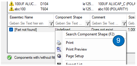
If no Essemtec part exists for a component group, right-click the row in the lower component table and select Search Component Shape (F2).
This allows the user to select an existing package or component shape from ePlace. PCB-Investigator can then create a new Essemtec part in ePlace using this selected shape.
PCB-Investigator only creates the new part. Missing component information must be completed later in ePlace by the user.
If no package is assigned, the component is still exported with the part name from the list. In that case, the part does not yet exist in ePlace and must be created later there. ePlace will warn the user about this situation.
Review the selected Essemtec part details
The lower table shows the selected Essemtec part or component shape for the currently selected component group. It contains information such as Essemtec name, component shape, comment, size values, processes, and pin analysis result.
Use the graphical preview
The preview on the right side overlays the CAD package and the selected Essemtec package or shape. It helps the user visually check body size, pin position, pin numbering, package center, and polarity.
The CAD and Essemtec outlines are shown together so that mismatches can be detected before export. If the Essemtec package is shifted or rotated compared to the CAD package, the component may not fit until the placement transformation is corrected.
Move or rotate the selected part
Use Move Part to shift the selected Essemtec part relative to the CAD component. The step width defines the movement distance for each click.
Use Rotate Part to rotate the selected Essemtec part. The rotation value is entered in degrees and is applied clockwise.
Use Reset Transform to remove the manual transformation and return to the automatically recognized position.
Enter the project name
The Project name is used as the base name for the created ePlace recipes and optional jobs.
Recipe names are created from the project name, the step name if required, and the side postfix. For the selected step itself, the project name is used unchanged as the base name. For lower-level steps, the step name is appended. The side postfix is then added, for example Top or Bot.
Select the export side
Use Top Side and Bottom Side to define which board sides are exported. Only the activated sides are created in ePlace.
The exporter creates separate recipes per side and step. For panels and family boards, the individual board recipes are created first. Panel-level recipes are then created separately and reference the corresponding individual board recipes in ePlace.
Select a template recipe
Press the template recipe selection button to select an existing ePlace recipe as a template. The selection dialog lists the available recipes from ePlace.
The selected template can be used to copy ePlace-specific settings into the newly created recipes. These settings are independent from the PCB layout data in PCB-Investigator.
The following template settings can be copied if selected:
Machine Settings
Process Control
Transport Parameters
Export fiducials
Activate Export Fiducials to export recognized fiducial pads to ePlace.
PCB-Investigator recognizes ODB++ pads on the outer copper layers with the attribute .pad_usage=l_fiducial or .pad_usage=g_fiducial. These pads are exported per step using the selected ePlace fiducial symbol.
The number in brackets shows the number of recognized fiducials that will be exported with the current settings.
Export bad board markers
Activate Export Badmarkers to export recognized bad board marker pads to ePlace.
PCB-Investigator recognizes ODB++ pads on the outer copper layers with the attribute .board_mark. The value of the attribute is not relevant. Pads with values such as bbm or gbm are recognized.
The pads are exported per step using the selected ePlace badmarker symbol. The number in brackets shows the number of recognized badmarkers that will be exported with the current settings.
Set an additional global rotation
Use Additional Rotation (CW) if the PCB is placed into the machine with an additional rotation.
The entered angle is applied globally to the generated recipe. The value is clockwise.
Check the recipe process order
The Recipe Process Order area shows the processes available from ePlace, for example Glue, Solder, and PICKANDPLACE.
The processes shown for each component come from ePlace. The user can select which processes are included and define their order before export.
Select the default medium for each process
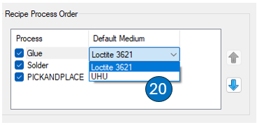
For each process, select a Default Medium from the list provided by ePlace.
The selected medium is required when the job or recipe is created in ePlace. The available names come from Essemtec/ePlace.
Create the recipe or recipes in ePlace
Press Create Recipe(s) in ePlace to create the required ePlace recipes from the current list and settings.
Before the export starts, PCB-Investigator checks whether the required recipe and job names are still available in ePlace. If one or more names already exist, the occupied names are displayed and the user must change the project name or naming settings before exporting.
PCB-Investigator does not delete, edit, or overwrite existing ePlace objects. It only creates new objects.
All components currently shown in the list are written to the recipe. Parts are only newly created in ePlace if they were not found during refresh/matching and if the user assigned an existing package or component shape.
Create jobs per side if required
Activate Also create a 'Job' per Side if jobs should be created together with the recipes.
A job is an ePlace object that is based on one or more recipes. If this option is active, PCB-Investigator creates the required jobs after creating the recipes.
Additional information: XML settings
Some naming options can be adjusted manually in the XML settings file:
%LOCALAPPDATA%\EasyLogix\PCB-Investigator\PlugIns\EssemtecExportSetting.xml
The default side postfixes are typically Top and Bot. They can be changed in the XML settings if another naming convention is required.
The name prefixes for exported fiducials and badmarkers can also be configured there. By default, fiducials use the prefix Fid and badmarkers use the prefix Bad. The generated names are therefore created as Fid1, Fid2, Bad1, and so on.