The plugin DFM Analysis can be found under the grid "Analysis" respectively "Assembly".
Here you will find six tab pages available for performing the DFM analysis: "Selective Soldering", "Fiducial Marker" (AOI verification), "Panelization" (technical verification of panels), "Testpoint", "Solder Paste" and "Trace Under Component". These single analysis functions are described below.
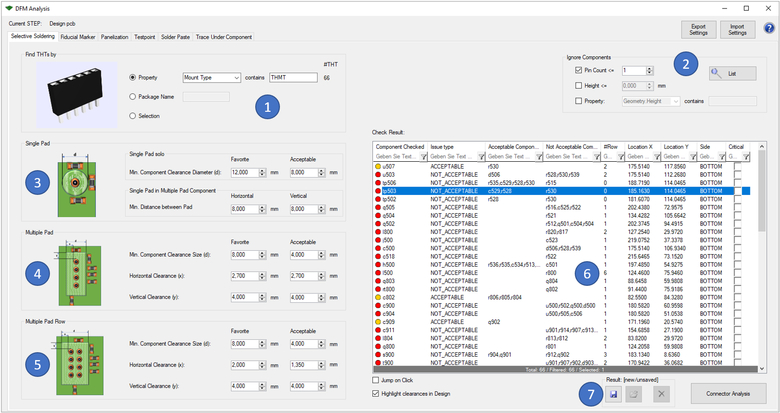
To begin with, the first topic is "Selective Soldering". This checks whether the set THT components will fit at the given location or whether the pins or holes of the THT component may be too close to components on the opposite side. The THT components you want to check can be selected either by the property or by the package name. It is also possible to directly select the THT components (1).
Before you can start the "Connector Analysis", you have to define the settings for the analysis. There is a distinction between "Single Pad" (3), "Multi Pad" (4) and "Multi Pad Row" (5). For each case, you can individually define the settings that will be used for the analysis. The pictures are intended to illustrate these variables. Each variable is determined by two different values, the "favorite" or optimum value and the "acceptable" value up to which manufacturability (according to your specifications) is still guaranteed.
The results of the analysis are then displayed in the table on the right-hand side of the window (6). Right-click to export them in HTML format. You can also use the tool to display the result. Components in the yellow area are located in the range you have defined as still acceptable. If a component is within the red area, the producibility with the current design is not guaranteed or the specifications defined by you are not fulfilled. Critical errors can also be marked for later use (e.g. in the 'Extended Design Report')
Following picture shows an example error of this analysis:
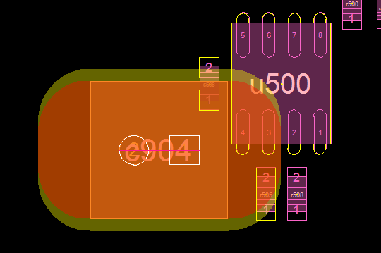
The THT component c904 is located on top side, but soldered on bottom side. The yellow marked components are too close to the soldered pins according to the 'Multi Pad' rule. The red area shows the "Acceptable" area, the yellow one is the "Favorite" area.
The following functionalities are equally integrated in all six options:
The "Fiducial Marker" analysis allows you to check whether the markers set for the AOI analysis can be implemented according to the selected specifications.

To do this, you must first search for the fiducials in your design (1). Four options, "Pad Usage", "Pad Geometry Name", "Package Name" and direct selection via the tool are provided for this purpose.
You can check the found fiducials for their manufacturability with 3 different parameters (3): "Copper Diameter", "SolderMask Diameter" and "Component Clearance Diameter". The check is then performed using these settings. Again, the results are displayed in the table on the right (4) or can be viewed directly via the tool. Critical errors can also be marked for later use (e.g. in the 'Extended Design Report').
The following functionalities are equally integrated in all six options:
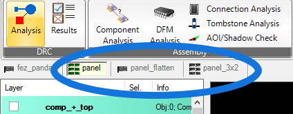
The "Panelization" option allows you to check whether your panel meets the specified measurements. In order to be able to start the analysis for the "Panel Dimensions", you must first switch to "panel" in the tool.
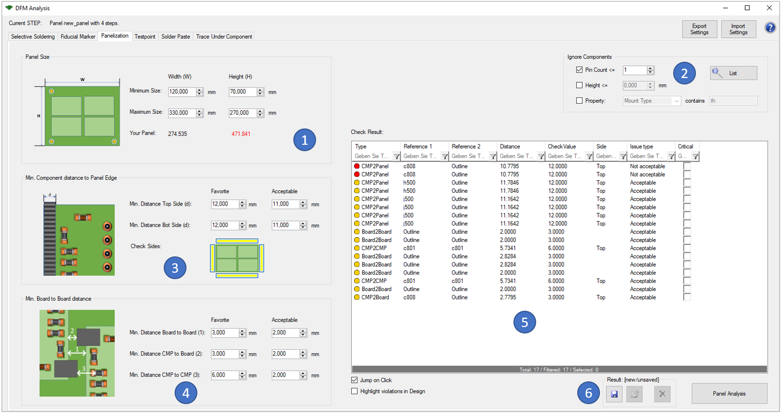
The size of the panel can be checked in the first block "Panel Size" (1).
You can also set the "Minimum Distance to Panel Edge" between components and the edge of the panel (3). At the same time, you have to choose an optimal value ("favorite") and a boundary value ("acceptable"). If the acceptable value is not reached, the producibility of the panel is endangered. Furthermore, you can decide, which edge of the board should be checked ("check sides").
Last you can analyze the "Board to Board distance" (4). Here the distance between boards, as well as the distance between component and foreign board, and component to component can be checked. Again you can enter an "Acceptable" and "Favorite" distance.
The results of the analysis are displayed in the window on the right (5). You can also view the analysis results directly in the tool. Critical errors can also be marked for later use (e.g. in the 'Extended Design Report').
Following picture shows an example error of this analysis:
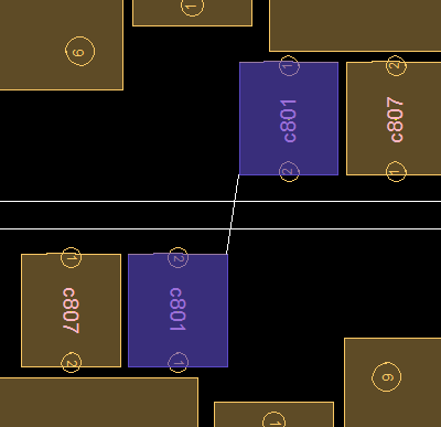
The component c801 of one board is too close to the same component on the neighbored board.
The following functionalities are equally integrated in all six options:
The "Testpoint" option allows you to check the distance between testpoints and between testpoint and components. This analysis is important to ensure e.g. the manufacturability of ICT adapters.
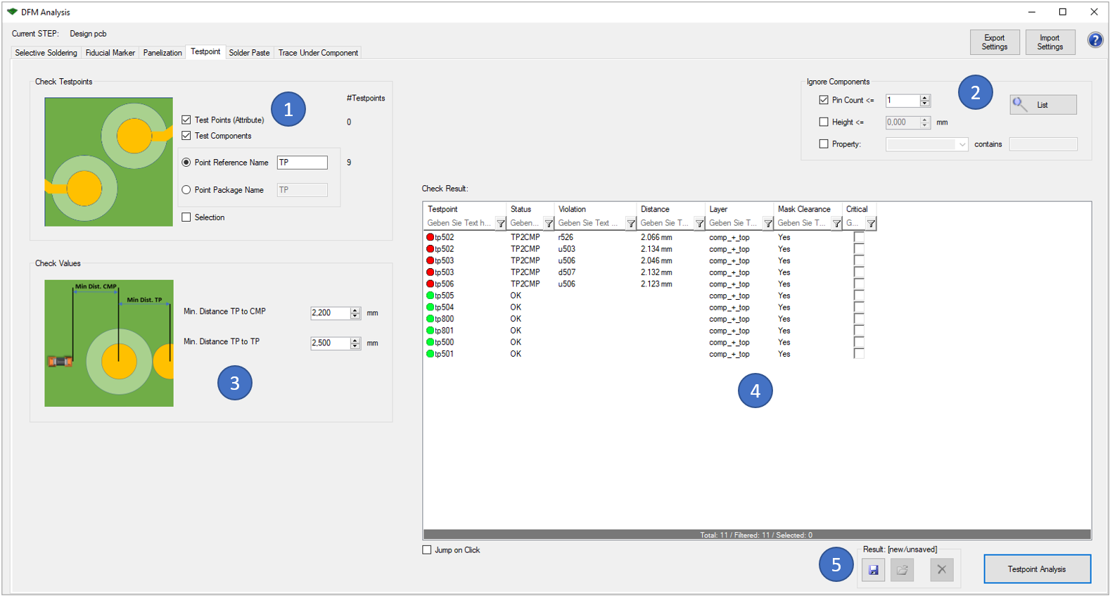
In the first block (1) there are different options to identify test points:
With the block "Check Values" (3), you can enter the wanted distances between testpoints (center to center) or between testpoint and components (center to outline).
The results of the analysis are displayed in the window on the right (4). You can also view the analysis results directly in the tool. Critical errors can also be marked for later use (e.g. in the 'Extended Design Report').
Following picture shows an example error of this analysis:
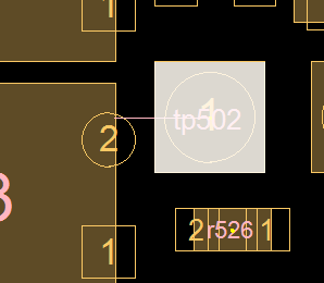
A component is too close to the test point tp502.
The following functionalities are equally integrated in all six options:
The "Solder Paste" option allows you to check if all component pins have a solder paste object, a copper pad, and a solder mask clearance defined and if the solder paste is inside a solder mask clearance.
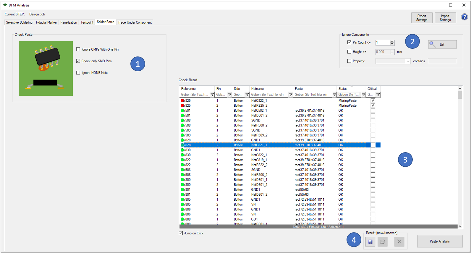
In the first block (1) you can define which components should be analysed. Here you have following ignore options:
The results of the analysis are displayed in the window on the right (3). You can also view the analysis results directly in the tool. Critical errors can also be marked for later use (e.g. in the 'Extended Design Report').
Following error types are reported:
The following functionalities are equally integrated in all six options:
The "Trace Under Component" option allows you to check, if certain components have unallowed copper tracks under their body between their pins. This is mostly unwanted for small 2-pin components, as it can cause problems during soldering.
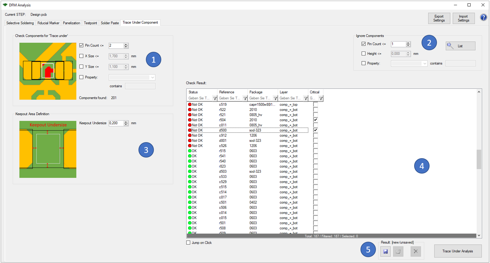
In the first block (1) there are different options to identify the components that should be analyzed:
With the block "Keepout Area Definition" (3), you can enter the wanted undersize that is used to determine the keepout area under the component body and between its pins.
The results of the analysis are displayed in the window on the right (4). You can also view the analysis results directly in the tool. Critical errors can also be marked for later use (e.g. in the 'Extended Design Report').
Following picture shows an example error of this analysis:
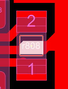
The component "r808" has unwanted copper tracks under its body inside the keepout area.
The following functionalities are equally integrated in all six options:
The plugin Component Analysis can be found under the grid "Analysis" respectively "Assembly".
Here you will find two tab pages available for performing the Component Analysis: "Component Distance Analysis" and "Component Placement Analysis". These single analysis functions are described below.
The "Component Distance Analysis" option allows you to check the distance between components and between components and the board outline. This analysis is important to ensure e.g. the manufacturability during the placement and soldering process.
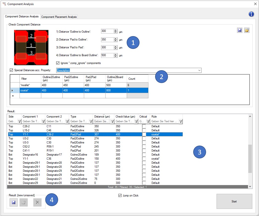
In the first block (1) you can define the different check values:
Here you also have the possibility, to ignore unplaced components (by ignoring components with a ".comp_ignore' attribute).
In the second block (2), you can define "Special Distances acc. Property". That means, you can define the same set of rules as in (1) but with different values for sub groups of components. The Filter is matching a literal string, but wildcards like " * " can be used to make more broad filter settings e.g. 0602*. The sub groups are build by a given component property. Examples are:
The results of the analysis are displayed in the window on the bottom (3). You can also view the analysis results directly in the tool. Critical errors can also be marked for later use (e.g. in the 'Extended Design Report').
With the buttons on the top right side of the window you can export the previously defined settings so that you can reuse them for later analyses. Already saved settings can be imported via the "Import Settings" button.
The last result can be saved and reloaded with the buttons on the lower left side (4). This stored result is also used in the 'Extended Design Report'.
Clicking on the question mark on the top right of the window opens the corresponding page of our online manual.
Following picture shows an example error of this analysis:
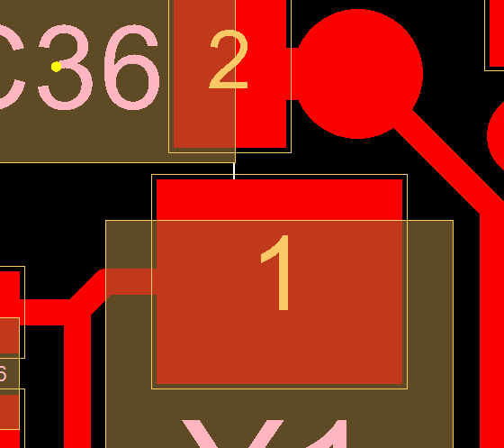
The copper pad of the X1-1 is too close the the component body of C36.
The "Component Placement Analysis" option allows you to check, if the MPN Package of a component fits the CAD Package.
A MPN Package (MPN = Material Part Number) is the real component outline of a part. This outline is often much smaller than the corresponding CAD package body. The MPN Package can also contain the contact surface of the pin. In this analysis, this contact surface of the pins is analyzed. You can define, where the contact surface has to be situated inside the copper pad.
A standard design has no MPN Package definitions included. EasyLogix offers the 'EasyLogix Part Library' (EPL) to add detailed part information like datasheets, MPN packages, 3D step files, ... to your design.
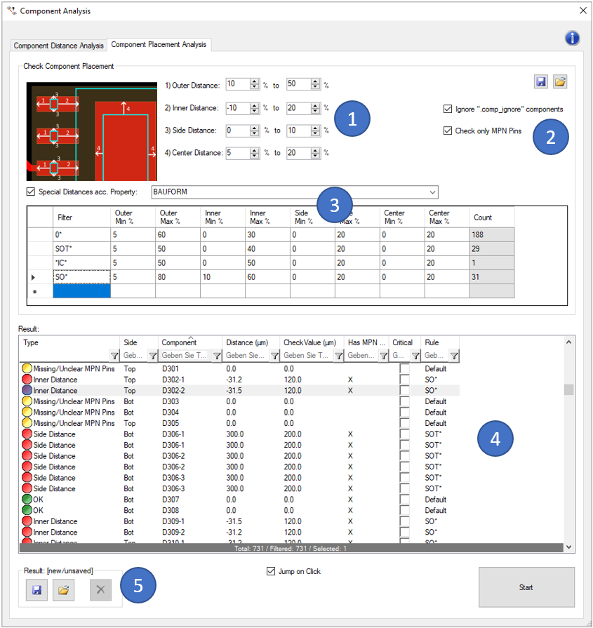
In the first block (1), you can define the different check values:
In the second block (2), you can define filters to ignore unplaced components (by ignoring components with a ".comp_ignore' attribute) and components without MPN package definitions.
In the third block (3), you can define "Special Distances acc. Property". That means, you can define the same set of rules as in (1) but with different values for sub groups of components. The Filter is matching a literal string, but wildcards like " * " can be used to make more broad filter settings e.g. 0602*. The sub groups are build by a given component property. Examples are:
The results of the analysis are displayed in the window on the bottom (4). You can also view the analysis results directly in the tool. Critical errors can also be marked for later use (e.g. in the 'Extended Design Report').
With the buttons on the top right side of the window you can export the previously defined settings so that you can reuse them for later analyses. Already saved settings can be imported via the "Import Settings" button.
The last result can be saved and reloaded with the buttons on the lower left side (5). This stored result is also used in the 'Extended Design Report'.
Clicking on the question mark on the top right of the window opens the corresponding page of our online manual.
Following picture shows an example error of this analysis:
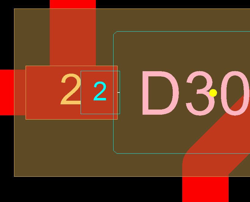
The contact surface of the pin 2 of the MPN Package for D30 is not matching the "inner distance" rule. That means in this case, the pin's contact surface is partly outside the copper pad. A reason could be, that the choosen part (MPN) does not fit to the CAD data. Soldering issues and failures are likely.
You can find the Testpoint Assign Tool under Plugin >> Assign Testpoint Attribute.
This tool helps to find and mark testpoints in a layout which could be defined via multiple non standardized attributes. Marking them with this tool then helps to standardize this and prepare the layout for following tools (for example the DFT Preperation).
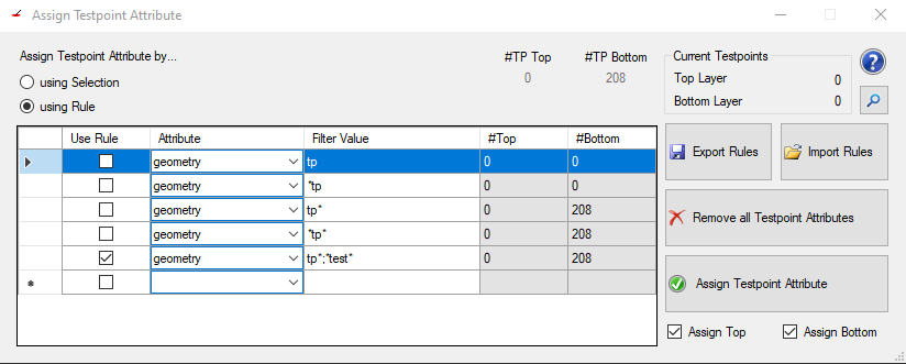
On the top left you can switch between using the current selection or a set rule to find the testpoints and assign the test_point value.
When choosing rules you can add another rule by checking the checkbox of the lowest row in the current listview and then fill out which attribute should be tested and what value needs to be set in said attribute.
All attributes are listed in a simple drop down menu. The Filter Value then has to represent the value of the attribute. Wildcards are allowed when searching for attribute values. The image shows for example all ways to search for "tp" in the "geometry" attribute:
Also it is possible to search for multiple values of the same attribute as shown in the last row. Simply seperate the values with a semicolon.
Boolean attributes do not need any value since their existance already means they are set.
To remove a rule simply select the whole row by clicking on the left most column of the row you want to delete (left of Use Rule) and press the "delete" key on your keyboard.
Checking a rule will select all found possible testpoints of the job (the checkboxes Assign Top and Assign Bottom change the selection depending on the check state of them)
On the top right side there is an information panel showing:
Export Rules exports the currently set rules to a xml file on selected location on the machine or in a cloud
Import Rules imports rules from a file either from the machine or from a cloud
Remove all Testpoint Attributes removes the "test_point" attribute from all pads of the job
Assign Testpoint Attribute adds the "test_point" attribute to either the currently selected pads or the pads found by the selected rule (handled by the radiobuttons "using Selction" and "using Rule")
Assign Top is a checkbox that when unchecked the "test_point" attribute will not be set for the pads on the top layer
Assign Bottom is a checkbox that when unchecked the "test_point" attribute will not be set for the pads on the bottom layer
To find possible testpoints the attribute histogram is a good way to start.
All Plugins have the following two Interfaces for direct calls from the outside.
///<summary
/// Analysis interface for scripts and plugins.
///</summary
→ The Header from the first Interface.
public interface IPCBIAnalysis {
///<summary
/// The name of this analysis to identify it with the settings.
///</summary
string Name { get; }
///<summary
/// The readable name of this analysis
///</summary
string Title { get; }
///<summary
/// The path to the results directory of this analysis relative to the job path
///</summary
string ResultsFolderName { get; }
///<summary
/// The preview icon for this analysis
///</summary
Icon PreviewIcon { get; }
///<summary
/// Set if the file preview should show if results are available
///</summary
Set if the file preview should show if results are available
///<summary
/// Create a instance of rules to define the default standard rules.
///</summary
PCBI.Automation.Rules.RulesContainer GetStandardRules();
// void AddToUpdateProgress(PCB_Investigator.PCBIWindows.PCBIWorkingDialog working, int minValue, int maxValue);
// bool Execute(string ResultFilePath);
public interface IPluginAnalysis: IPlugin, IPCBIAnalysis{
///<summary
///
///</summary
///
void AddToUpdateProgress(PCB_Investigator.PCBIWindows.PCBIWorkingDialog working, int minValue, int maxValue);
bool Execute(IAnalysisParams analysisParams);
bool Execute(string resultFilePath); }
→
The script is allowed to increment
values between minValue and maxValue.
Watch our PCB-Investigator - DFT Preperation Video here:
Tutorial: DFT Preperation & Machine Export: