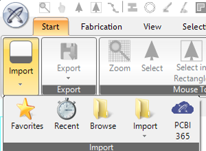
To load a new design or job, click on the “Import” button.
Here, you can choose between
• designs that you have marked as a favorite (“Favorites”),
• recently opened jobs (“Recent”),
• specific files in your data via the “Browse” function,
• an empty design via "Import” or,
• a design via our cloud platform PCB-I 365 (if you are using this service).
Alternatively, you can simply drag & drop your files into PCB-Investigator to open them.
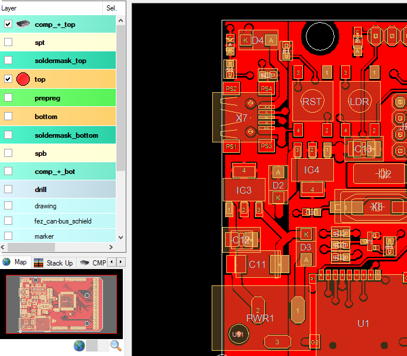
The layer stackup of your currently opened design is displayed on the left side of the main window.
To show or hide layers, check or uncheck the corresponding layer.
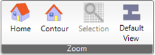
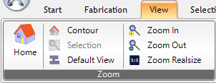
By clicking on "Default View" (under the zoom function in the toolbar at the top), all layers are hidden at once. Only the contour of your design will be visible.
The “Zoom” option allows you to view your design in more detail. The small window below the stackup, showing you a miniature version of your design, serves as an orientation aid. Here, you can see by means of the red rectangle at which point in the design you are currently working.
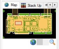
To see or work on specific parts of your design, use the scroll function of your mouse to zoom in towards the corresponding position. You can also use the small window on the left side of the start window to zoom. Simply select the point of the design you want to view more closely by dragging a rectangle to the corresponding position.
If you want to display the design in its original size again, press the "Home" button at the top of the toolbar. Alternatively, you can select "View" in the ribbon above. Likewise, different zoom options are offered here, such as zooming in and out or displaying the "Home" screen showing the full design.
To change the matrix / layer stackup, you have to open the “Fabrication” tools in the above ribbon
to open the matrix.
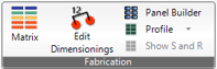
or right-click on the layer stack-up (left side).
The following matrix dialog will open:
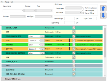
By clicking on the corresponding layer, you can change various parameters of this layer, such as layer name, context, type, layer thickness or polarity. By clicking on the blue arrows on the right side of the window, the position of the selected layer can also be changed by shifting.
To add a layer, click on "Edit" and select "Add Layer" to choose the type of layer. Drill layers are added specifically with "Add Drill Layer".
To save the changes, click on "File" and "Save Matrix". Otherwise, you will be asked to save your changes when closing the window.
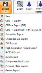
To save changes to a design, select "Export" in the ribbon at the top. You can choose the type of file format, like ODB++, you would like to use to save and export your design. All available file formats PCB-Investigator supports are listed here for you to choose from.
To add data, you can basically use the Import button or drag & drop.
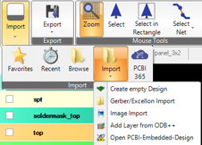
Here, you will find numerous import options. For example, you can use CSV Components to import only components, or additional layers, additional information (attributes), netlists or entire designs.
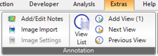
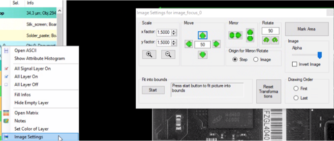
Images can also be loaded via the "Extras" button.
Use the “Image Settings” for adjusting. This serves e.g. the better processing of Gerber files by an enhancement on the basis of illustrations.
To load Gerber files, use the import function or drag & drop analogously to loading other jobs. To be able to fully use Gerber for analyses with PCB-Investigator, we offer you some processing options. To "complete" Gerber files with drill holes, upload the corresponding Excellon file. In addition, the layer stackup needs to be
defined (using the matrix) and possibly, for completion, the components are to be uploaded by means of a CSV file. Deviations in the overlay of layers can be adjusted using "Transform Layers“.
![]()
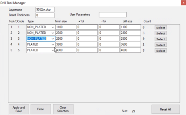
Using the Drill Tool Manager (Right-click on the layer stackup after a drill layer has been selected),
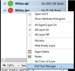
you can define drill holes as plated and unplated (e.g. to perform a DRC analysis).