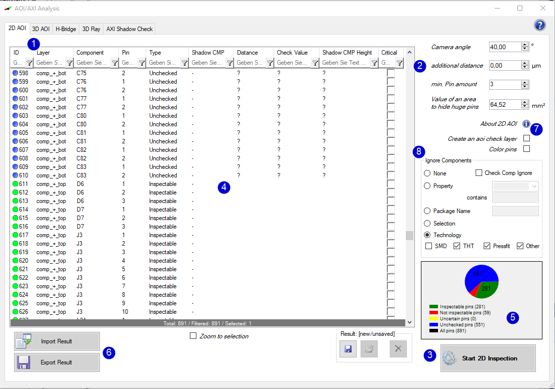
By using the 'AOI check' button the following window appears:
Open a PCB design first and then start the ‚AOI check‘.
First you have to decide, if you want to analyze your design with a 2D or 3D inspection. However, the following section deals only with 2D inspection. If you need information about the 3D inspection, use the 3D AOI description.
Enter the angle of your future automated optical inspection for the camera angle. Tolerances can be calculated using’ additional distance’. By default, this value is set to 0.00. As 2-pin components often aren´t relevant or, due to their shape, difficult to analyze , they can be excluded here. Occasionally components with very large pins are used. These pins often do not need to be checked due to their size. For this reason, enter an area in the’ Value of an area to hide huge pins’ input field that meets your requirements. You can also select the two options’ Create an aoi check layer’ and’ Color pins’. If you want an additional layer, on which the direction of inspection per pin is marked, activate ’Create an aoi check layer’.With the use of the ’Color pins’ option, the pins in the diagram displayed in color are also colored in the design.
After you have adapted all values to your requirements, you can start the inspection.
The inspected components and their pins are now displayed and can be sorted using the riders. The result list contains one line per pin. It contains the following information:
ID: Identification Number
Layer: Contains on which side the pin can be found
Component: Component name
Pin: Pin number
Shadow Component: Component that is too close to the pin
Distance: Shows the calculated distance
Checkdistance: Shows the required distance
Shadowcomp. Height: Shadow component height
The diagram illustrates the result of the inspection.
The inspection can now be saved using the ’Export Result’ option. When using the import result, an old inspection result can be loaded.
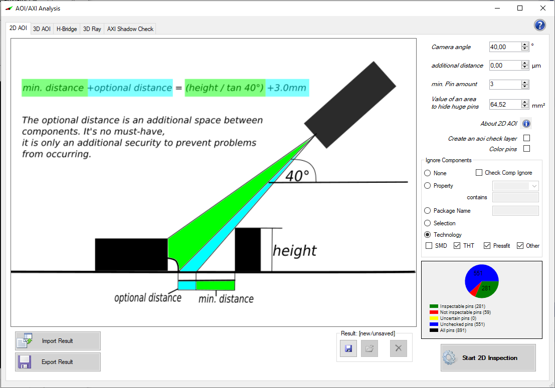
If you move the mouse over the ’Help’ icon, the following picture will be displayed to explain how 2D inspection works.
Ignore components: At this point you have the option exclude components that are not relevant for the later AOI analysis. Depending on your design, you can do this by using the properties, the package name or by individually selecting the components in the tool itself.
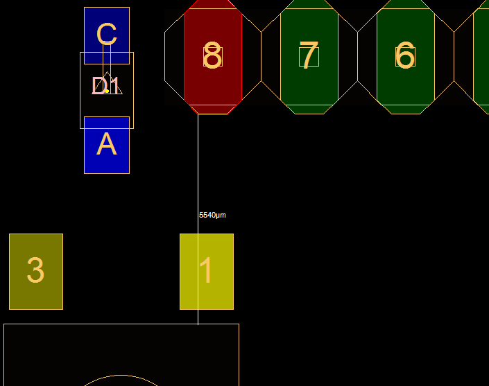
Example:
Doubleclick an entry shows the component J1 and the corresponding pin 8 (red colored) with too small distance to the component LDR after the 2D inspection.