AOI Analysis 3D

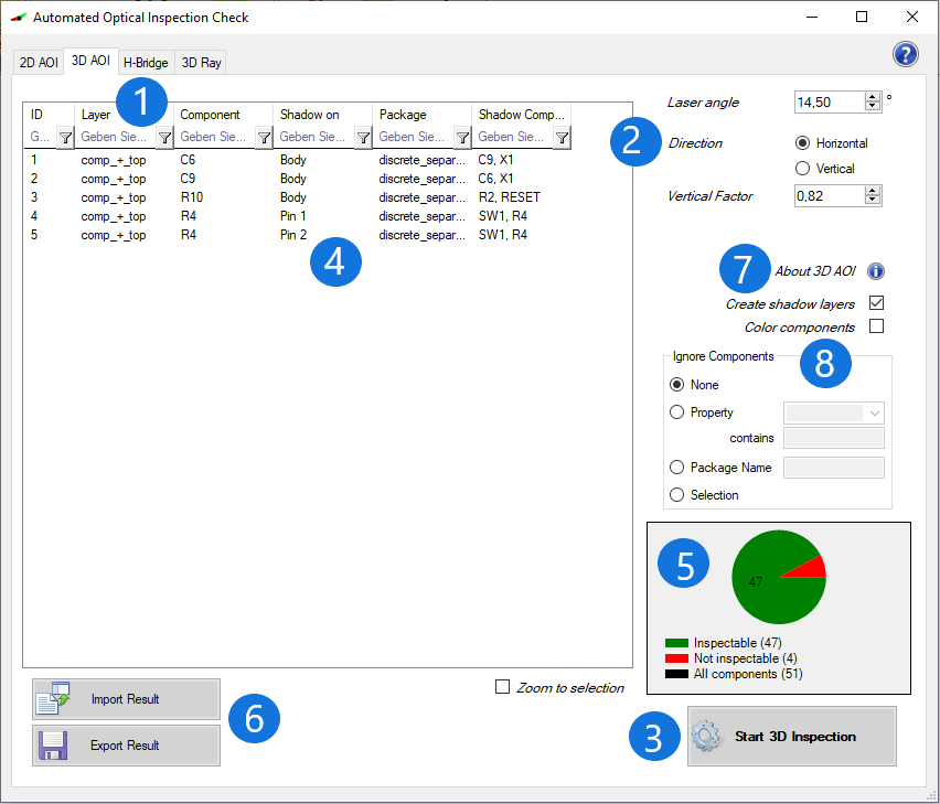
By using the 'AOI check' button and switching to 3D AOI the following window appears:

Open a PCB design start, then the ‚AOI‘.

  1. First you have to decide,if you want to analyze your design with a 2D or 3D inspection. However, the following section deals only with 3D inspection. If you need information about the 2D inspection, use the 2D AOI description.
  2. First replace the’ laser angle’ arranged between the laser and the camera with its actual laser angle. Since the direction the laser head moves in differs during the 3D inspection, it can also be adjusted with ’horizontal’ and ’vertical’. The colouring of the affected components can be selected as required. It is also possible to graphically display the overlapping of the shadow with other components in separate layers using the’ create shadow layers’ option. So the layers show the shadow of a component in both test directions and are shown as follows.


aoi_3d_additional_layer

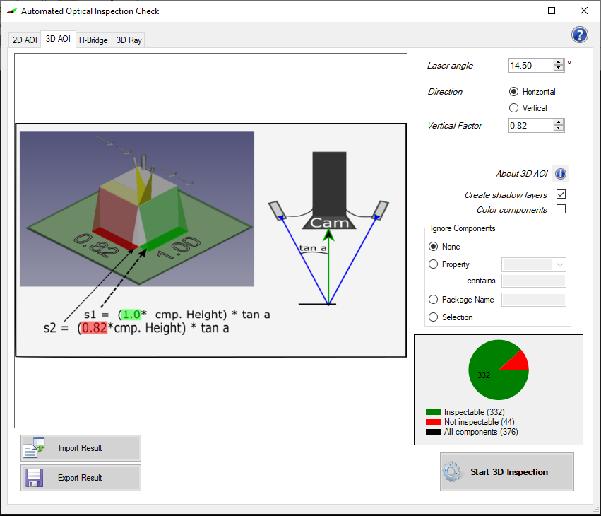
3. After you have adapted all values and selection options to your requirements, you can start the inspection

4. The inspected components and their pins are now displayed and can be sorted using the riders. The result list contains one line per pin. It contains the following information:

    • ID: Identification Number
    • Layer: Contains on which side the pin can be found
    • Component: Component name
    • Shadow on: Identifier whether the shadow falls on a component body or the corresponding pin
    • Package: Package name
    • Shadow Components: Shows the component names of the components affected by the shadow

5. The diagram illustrates the result of the inspection.

6. The inspection can now be saved using the ’Export Result’ option. When using the import result, a past inspection result can be loaded.

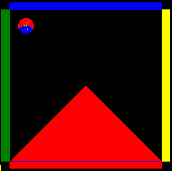
7. If you move the mouse over the ’Help’ icon, the following picture will be displayed to explain how 2D inspection works.

8. Ignore components: At this point you have the option exclude components that are not relevant for the later AOI analysis. Depending on your design, you can do this by using the properties, the package name or by individually selecting the components in the tool itself.
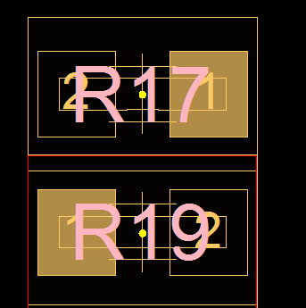
Example:
Doubleclick an entry shows the component J1 and the corresponding pin 8 (red colored) with too small distance to the component LDR after the 2D inspection.
aoi_3d_list_entry_on_board