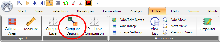
To compare graphically, you can either start "Compare Designs" via PCB-Investigator or you can start it as a Desktop-App, called "PCB-Investigator-Graphic-Board Compare".

Starting "Compare Designs" or "Graphic-Board-Design", it will result in the same dialog. After the tool has been started, it will look like this.
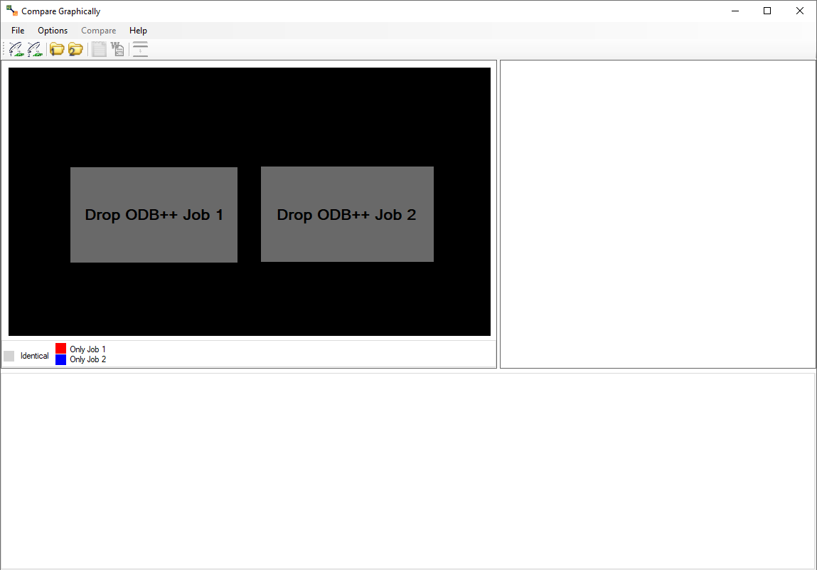
To compare two jobs, you have to add to new designs.
The two currently selected designs are mapped to colors.
![]()
After choosing the second design, the following dialog will open automatically.

(You can also open this dialog by clicking this button or using the "Compare" tab.)


The first opened dialog will change and will now look like the following picture (only if there are results).
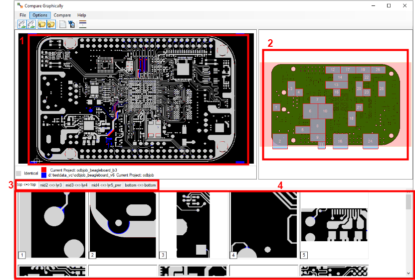
To simplify the dialog, it can be splitted into four different views.
The following GIF´s show what the four areas can be used for.
View 1 + 2:Â

View 3 + 1:

View 4 + 2 + 1:

Â
Further details:
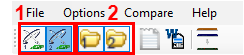
1. Using the "File" tab, you can create different reports of the comparison. The following report formats are available.
The HTML Report may be the best report for visualization reasons. The report looks like this:

2. The "Options" tab allows the following opportunities.

1. The "Tolerance" option allows you to adjust the difference the PCB elements of the two layers may have. (Smaller values cause a higher computing time.)
2. The second option "Show PCB-Investigator" opens two instances of PCB-Investigator. Each instance uses one of the chosen designs. Position it side by side to compare it directly. Using the tiles of the main window, the two instances will also zoom in the chosen tile.
3. The option "Activate Layers" and "Deactivate Other Layers" are just influencing the second option "Show PCB-Investigator". Activating them will cause to have a difference in the seperated two PCB-Investigator instances.
Command Line Arguments (Avalable with Version 16 or beta V 15.1):
first and second arguments have to be pathes to the compare designs
-in_profile_only=true
-export_report_path=D:\\output\\example.html
-check_all_layers=true
Example call as batch file:
D:\tmp\PCB-Investigator-Beta\GraphicBoardCompare.exe D:\Data\compare\job1 D:\Data\compare\job2 -in_profile_only=true -check_all_layers=true -export_report_path=D:\tmp\compare.html