
Now that you are familiar with the workspace, you can begin exploring the PCB.
The visibility of the PCB layers is controlled in the Layers area.
Show or hide individual layers to focus on the structures that are relevant to your current task.
Tip For your first steps, enable the Top Copper and Top Component layers to get a clear overview of the PCB layout.

Use the following mouse controls to navigate through the design:
The Start tab provides several view controls in the Zoom panel.
Use Home to display the complete PCB. You can then zoom in and focus on a specific area of the design.
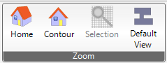
Tip Use Default View whenever you want to reset the current layer visibility and return to a simplified board outline.
The overview window below the Layers area displays a miniature view of the complete PCB.
The highlighted rectangle indicates the section currently visible in the main workspace.
Use this overview to keep your orientation when working with a highly zoomed-in section of the PCB.

Tip PCB-Investigator also supports Mouse Strokes for quick gesture-based commands while holding the middle mouse button. This optional feature is not required to complete this guide. See Mouse Strokes for details.
The complete PCB is visible, and you can zoom and pan through the layout.