
Start by downloading and installing the latest version of PCB-Investigator.
Tip If you already use PCB-Investigator, sign in with your existing credentials.
PCB-Investigator is installed, and you are signed in.
For your first steps, we recommend opening one of the integrated Demo Designs. This allows you to follow the guide without preparing your own PCB data.
The selected Demo Design opens in the main workspace.

You can also open your own PCB data:
Alternatively, drag and drop the files directly into the PCB-Investigator window.
PCB-Investigator supports a wide range of PCB and manufacturing data formats. See Supported Formats for a full list.
The PCB is open and displayed in the main workspace.
PCB-Investigator provides measurement tools for checking dimensions, distances, and clearances directly in the PCB layout.
Open the Start tab and click the Measure button.

Choose the measurement method that matches your task, then select the relevant points or objects in the PCB layout.
Typical measurement tasks include:
The exact workflow depends on the selected tool. See Distance Measurement for detailed instructions.
You have completed a basic measurement directly in the PCB layout.
After locating components, you can examine the electrical connections in the PCB design.
PCB-Investigator allows you to select a net directly in the layout or search for a known net by name.
First, switch to the appropriate net selection mode:
PCB-Investigator highlights the complete net, allowing you to follow its path through the design.

You can also use the Quick Search when you already know the net name:
%) and enter the net name, for example %GND.The corresponding net is selected and displayed in the PCB layout.
Tip
Net highlighting is useful for tracing signals and understanding the electrical connections between components.
A complete electrical net is selected and can be followed through the PCB design.
Before working with the PCB, take a moment to become familiar with the main areas of the PCB-Investigator workspace.
The application is divided into four main sections.

The ribbon at the top of the window provides access to commands and tools.
Functions are grouped into tabs such as Start. Additional tabs may be available depending on the installed edition, modules, and active workflow.

The Layers area on the left side displays the layer stack of the current PCB.
From here, you can:

The lower-left area contains additional tabs for design-related information and tools.
For example, the Properties tab displays information about selected PCB objects, while the CMPs tab provides access to the component list.
The available tabs may depend on the loaded design and active functions.
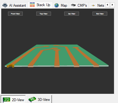
The central workspace displays the PCB layout.
This is where you navigate through the design, select objects, inspect structures, and perform analyses.
Tip The individual areas can be resized to provide more space for the PCB layout or additional information.
You know where to find the main controls, PCB layers, additional tabs, and the PCB layout.
After navigating to an area of interest, you can select individual objects in the PCB layout.
PCB-Investigator allows you to work with different PCB objects, including components, pads, traces, vias, and polygons.
Before selecting an object:

Click an object in the PCB layout.
The selected object is highlighted, making it easier to identify within the design.
Try selecting different objects, such as:
Notice how the selection changes depending on the object below the mouse cursor.
Tip If multiple objects overlap at the same position, click repeatedly to cycle through the available objects. Use separate clicks rather than a double-click. This applies to PCB objects other than components.
To clear the current selection, use the corresponding command in the context menu or the Clear Selection button in the toolbar.
PCB-Investigator keeps a history of recent selections. Use Previous Selection repeatedly to move back through them.
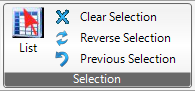
An individual PCB object can be selected, cleared, or restored from the selection history.
Now that you are familiar with the workspace, you can begin exploring the PCB.
The visibility of the PCB layers is controlled in the Layers area.
Show or hide individual layers to focus on the structures that are relevant to your current task.
Tip For your first steps, enable the Top Copper and Top Component layers to get a clear overview of the PCB layout.

Use the following mouse controls to navigate through the design:
The Start tab provides several view controls in the Zoom panel.
Use Home to display the complete PCB. You can then zoom in and focus on a specific area of the design.
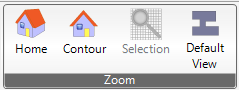
Tip Use Default View whenever you want to reset the current layer visibility and return to a simplified board outline.
The overview window below the Layers area displays a miniature view of the complete PCB.
The highlighted rectangle indicates the section currently visible in the main workspace.
Use this overview to keep your orientation when working with a highly zoomed-in section of the PCB.

Tip PCB-Investigator also supports Mouse Strokes for quick gesture-based commands while holding the middle mouse button. This optional feature is not required to complete this guide. See Mouse Strokes for details.
The complete PCB is visible, and you can zoom and pan through the layout.
You have completed the PCB-Investigator Quick Start Guide and are now familiar with the essential workflow.
Continue with the following topics to explore features that are relevant to your work.
The available functions depend on your PCB-Investigator edition, installed modules, and ribbon configuration.