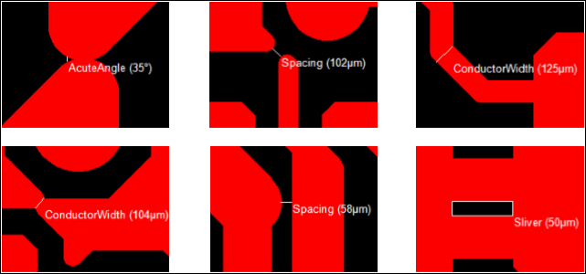

The result explanations help you to easily interpret the check results reported by PCB-Investigator`s Design Rule Check.
There is a focus on illustrating the technical background as well as on giving a understanding of the unavoidable tolerances during the PCB manufacturing process.

Small distances in copper, as well as thin copper areas might not be producible due to physical etching restrictions.
A chosen technology e.g. IPC Class II should be applied everywhere on the board, as only a single violation forces the PCB supplier to switch to finer production parameters (e.g. IPC Class I) for the whole board.
The finer the structures, the more expensive the board will be.

Solder resist webs with a width of less than app. 70µm are hardly producible with standard technology.
There is always the risk, that those small pieces will detach and adhere somewhere else, which can lead to solder problems and failures.
Smaller distances and webs might only be producible with an expensive special solder resists and less resist height, which influences the isolation quality.
To avoid unnecessary costs, PCB-Investigator reports all those violations.
 CAD data
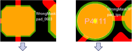
  With allowed displacement
 As there will always be a slight displacement between the solder resist and the conductive pattern, surrounding copper should have a minimum distance of the allowed displacement from the solder resist opening. If not, there is the risk that the surrounding copper will also be exposed, which can lead to electric shorts by e.g. solder bridges.
The allowed displacement is app. 75µm, also 50µm is possible, but more expensive.
 CAD data
  With allowed displacement
 The displacement can also have negative impact on the solderability of SMD pads or testability of test points.
To ensure further processability, there should be a solder resist opening with an oversize of the maximum allowed displacement (e.g. 75µm) for all SMD pads and test points.
So, the copper will always be completely solderable/testable.

Each drill should have a solder resist opening, which ensures that the drill is free of solder resist despite the combined displacement of the solder resist and of the drill itself.
A partly covered drill or solder resist in the drill sleeve can detach and adhere somewhere else during the cleaning process. This can lead to solder problems and failures and contaminates the chemical baths of the PCB supplier. It also effects the EMC behavior.

A completely covered drill without any solder resist opening on one side can´t be cleaned and therefore contaminates the chemical baths.
If covered on both sides, the enclosed air in the drill could break the solder resist cover when expanding due to heat. The result is unwanted dirt on the board.

The drill diameter and the drill distance are very important factors for the price calculation.
Very thin drills have a short life period and must often be replaced. They are also less long, which forces the PCB supplier to drill only 1-2 panels at the same time instead of drilling e.g. 5 panels in a package.
Small distances between two drills increase the risk the drill is breaking or the two holes are merging to one undefined shape.
Two holes at the same location can also lead to broken drills or an undefined hole shape.

To achieve a clearly defined connection between layers, the copper pads for the single drills must be large enough, so that a drill displaced within the allowed tolerances is still located completely within the pad.
If not, this can have a strong impact on the EMC behavior and lead to failures due to a loose or broken contact.
Small annular rings and therefore narrow tolerances in the drilling process might still be producible, but force the PCB supplier to use high-end drilling machines and to drill only one Panel at the same time instead of e.g. 5 panels in a package. This has a very strong influence on the PCB costs.

In this case we must differ between plated and un-plated drills.
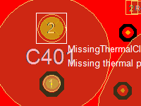
For plated drills, the distance to surrounding copper is important on inner layers, when the copper pad is omitted. Due to the production tolerances, the displacement of the drill could lead to broken connections or shorts, if surrounding copper is too close.

For unplated drills, the distance is needed for tenting the hole during the plating process to avoid copper in the hole. When the un-plated drill could not be securely tented, a second drill process after the plating process is needed instead. This raises the costs enormously.


Summary
Performing the Design Rule Check (DRC) of PCB-Investigator is the first step to avoid unneeded costs and to increase the reliability of your PCB.
Although in some cases the standard rules must be violated to fulfill some requirements (e.g. Space requirements), there is always a potential to save money and increase the reliability with a few minor layout changes.