With the help of the "Rule File Manager" different rule sets can be created and managed.
New: Save: Delete: Import: Export: Tolerance: Unit Converter: Compare:
Single check rules:
Outer Signal Rules
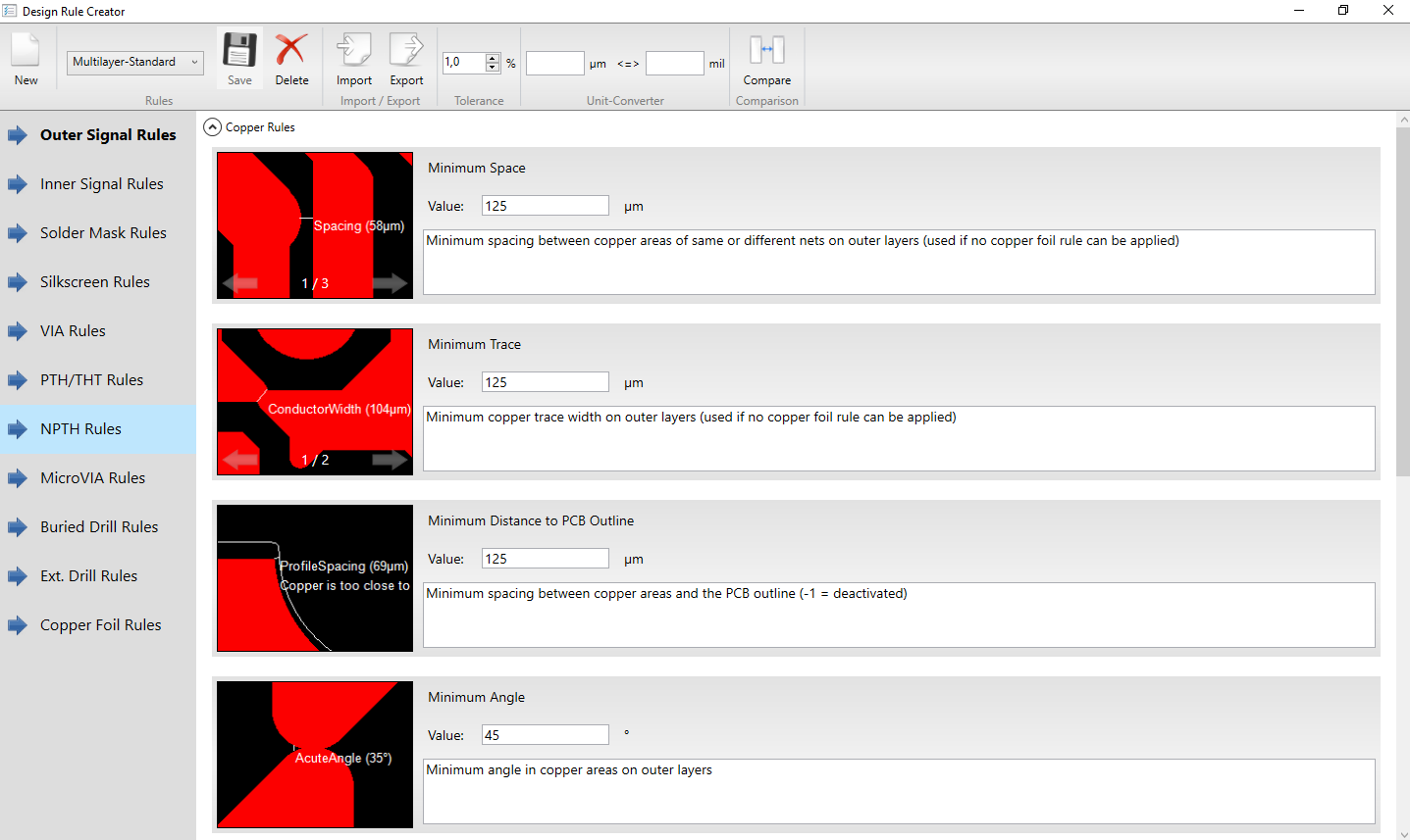
Minimum spacing between copper areas of same or different nets on outer layers (used if no copper foil rule can be applied)
Minimum copper trace width on outer layers (used if no copper foil rule can be applied)
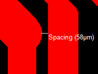
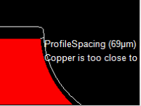
Minimum spacing between copper areas and the PCB outline (-1 = deactivated)
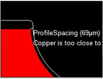
Minimum angle in copper areas on outer layers
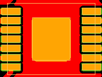
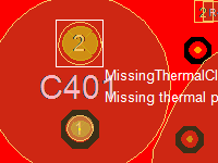
If active, all SMD pads with soldermask opening and component pin are reported, if they are located completely inside a copper area (no thermal reliefs)
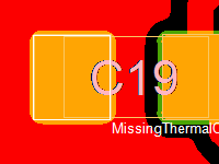
Do not report missing thermal pads, which are located completely under a component body and have a size larger as this value (e.g. cooling pads)
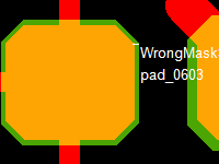
Minimum needed solder mask clearance arround SMD pads (.smd Attribute)
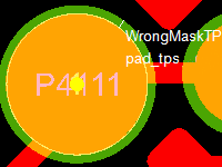
Minimum needed solder mask clearance arround test point pads (.test_point Attribute)
Inner Signal Rules
Minimum spacing between copper areas of same or different nets on inner layers (used if no copper foil rule can be applied)
Minimum copper trace width on inner layers (used if no copper foil rule can be applied)
Minimum spacing between copper areas and the PCB outline (-1 = deactivated)
Minimum angle in copper areas on inner layers
Solder Mask Rules
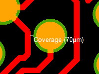
Minimum distance from the solder mask opening to surrounding copper
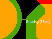
Minimum spacing between solder mask clearances (=smallest solder resist fillet)
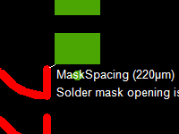
Minimum width of solder mask clearances
Minimum angle in solder mask clearances
Silkscreen Rules
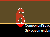
Minimum distance to any solder mask opening
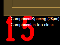
Minimum distance to any component
Check only text primitives (.nomenclature attribute) for a minimum distance to components, or all primitives
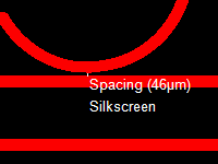
Minimum spacing between silkscreen printings
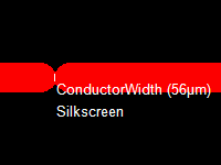
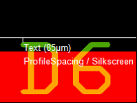
Minimum size of silkscreen primitives
Minimum spacing between silkscreen printings and the PCB outline (-1 = deactivated)
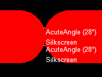
Minimum angle in silk screen printing
VIA Rules
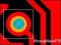
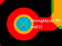
Minimum needed solder mask clearance for plated through holes (.drill=via)
Minimum needed solder mask clearance for plated through hole copper pads (.drill=via)
If active, mask clearances which are smaller than the VIA-Pad are not reported
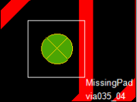
If active, missing solder mask openings for VIA drills will not be reported
If active, missing solder mask openings for VIA drills will not be reported
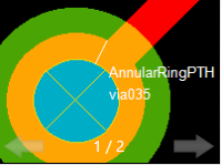
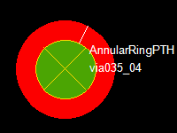
Minimum annular ring for the VIA on outer signal layers
Minimum annular ring for the VIA on inner signal layers
If active, missing copper pads on inner signal layers will not be reported
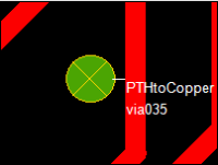
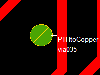
Minimum distance to surrounding copper on inner layers, if missing pads are accepted
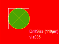
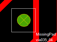
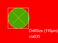
Minimum diameter of plated through holes (.drill=via)
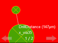
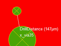
Minimum Distance to any other Drill
PTH / THT Rules
Minimum needed solder mask clearance for through hole technology drills (.drill=plated)
Minimum needed solder mask clearance for through hole technology copper pads (.drill=plated)
Minimum annular ring for the through hole technology drills on outer signal layers (.drill=plated)
Minimum annular ring for the through hole technology drills on inner signal layers (.drill=plated)
If active, missing copper pads on inner signal layers will not be reported
Minimum distance to surrounding copper on inner layers, if missing pads are accepted
If active, all THT copper pads are reported, if they are located completely inside a copper area (no thermal reliefs)
Minimum diameter of through hole technology drills (.drill=plated)
Minimum Distance to any other Drill
NPTH Rules
Minimum needed solder mask clearance for unplated through holes (.drill=non_plated)
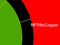
Minimum distance to surrounding copper on outer signal layers
Minimum distance to surrounding copper on inner signal layers
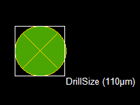
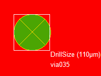
Minimum diameter of unplated through holes (.drill=non_plated)
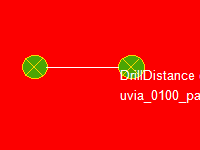
Minimum Distance to any other Drill
MicroVia Rules
Minimum needed solder mask clearance for laser drills
If active, missing solder mask openings for laser drills will not be reported
Minimum annular ring for the laser drill on all affected signal layers
Minimum diameter of laser drills
Minimum Distance to any other Drill
Buried Drill Rules
Minimum annular ring for the drill on outer signal layers
Minimum annular ring for the drill on inner signal layers
If active, missing copper pads on inner signal layers will not be reported
Minimum distance to surrounding copper on inner layers, if missing pads are accepted
Minimum diameter of plated through holes
Minimum distance to any other Drill
Ext. Drill Rules
Minimum Distance from THT to THT Drill
Minimum Distance from THT to VIA Drill
Minimum Distance from THT to NPTH Drill
Minimum Distance from THT to MicroVIA Drill
Minimum Distance from THT to Buried Drill
Minimum Distance from VIA to VIA Drill
Minimum Distance from VIA to NPTH Drill
Minimum Distance from VIA to MicroVIA Drill
Minimum Distance from THT to Buried Drill
Minimum Distance from NPTH to NPTH Drill
Minimum Distance from NPTH to MicroVIA Drill
Minimum Distance from NPTH to Buried Drill
Minimum Distance from MicroVIA to MicroVIA Drill
Minimum Distance from MicroVIA to Buried Drill
Minimum Distance from Buried to Buried Drill
Copper Foil Rules
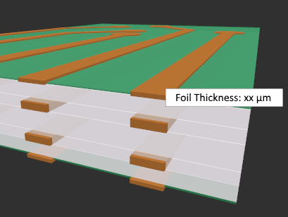
Maximum Foil thickness for this rule
Minimum spacing between copper areas of same or different nets on outer layers with this foil
Minimum copper trace width on outer layers with this foil
Minimum spacing between copper areas of same or different nets on inner layers with this foil
Minimum copper trace width on inner layers with this foil