

To change e.g. the order of layers, you have to open the "Layer Matrix" menu, which can either be directly accessed through right-clicking in the layer panel and selecting "Open Matrix" or selecting "Fabrication » Matrix" in the main menu. There you are able to i.a. add new layers, load predefined standard stack ups, and even print a report of your stack up or export it as CSV.
In addition to the order of the individual layers every other information like default stackup, layer type, hights, layer attributes, material, colour, etc. can also be adjusted to fully fit your needs. Once every configuration is in order the printed curcuit board can thoroughly be inspected by selecting one or more layers (by simply clicking on them) for visual representation. By default, each layer is assigned a specific colour so that it can quickly be identified which parts and layers are belonging together. Related colours and layers can be found between the checkbox and the layer name. Should the colours not meet your preferences, they can also be adjusted either seperately through right-clicking on the concerning layer and selecting "Set Color of Layer" or globally through "Start » Setup Colours".
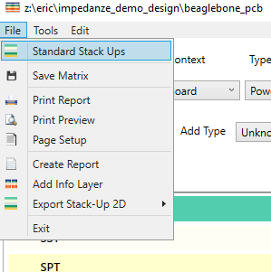
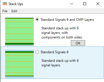
For example, you can choose a standard stackup for your pcb. To do so, right-click on "File" in the upper left corner of the menu. There, you have the option to choose one of the default stackups.
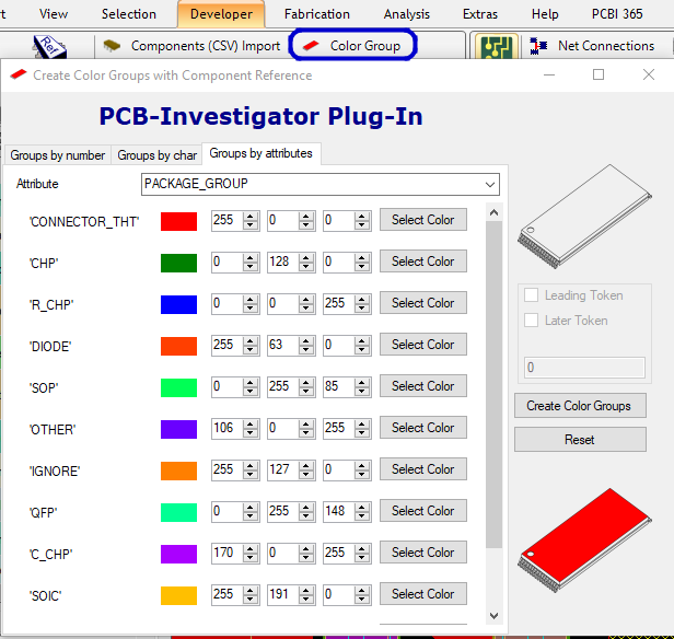
You can get to Colour Group via Developer » Color Group.
In both cases the colour scheme can of course be customised to fit your preferences.
Here is an example how it can look for package group coloring:

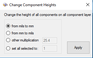
Component height is an important component property that is deeply attached to it. In earlier versions of ODB++ this property was just a number without unit. Since PCB-Investigator needs a unit for certain features like the 3D visualisation it assumes the unit "mils" by default. The Change Component Heights dialog which can be reached by Developer » Component Heights is a fail-safe that allows you to change the unit if it is falsely assumed by the program. Please note that this option only affects the component height property.
With the Filter option you can handle components only on active layers, only selected components or all components.
The netlist is an integral part of the inner workings of PCB-Investigator and thus the Generate Netlist function is of utmost importance and is needed especially in two main cases:
Note: You need correct stackup and drill information to generate the net list correct.
The NetGroup Wizard can be used to create net groups and to add or remove nets to them.
Open the NetGroup Wizard with clicking the "Net Groups" button.
The following dialog will show up.
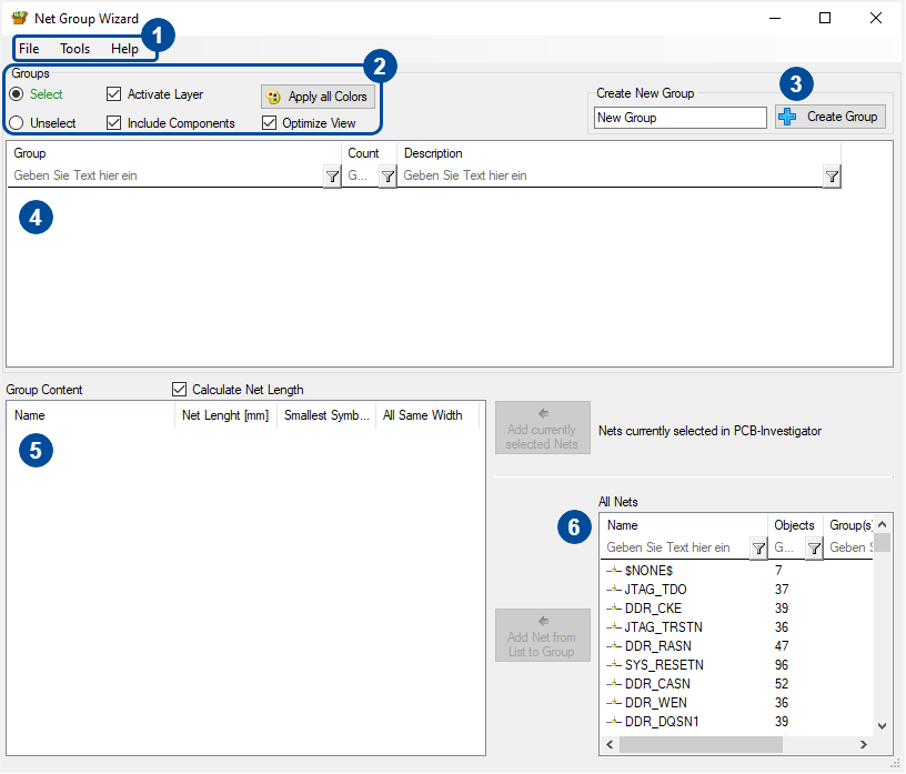
1. The two important tabs contain the following options.
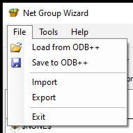
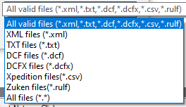
The net groups are always stored within the ODB design. Sometimes, you want to import net groups from another design. Prior to that, export the current net group to have a backup of them. In the import you can select between different file formats (xml, txt, dcf, dcfx, csv, rulf) to add net groups from other software (e.g. Xpedition or Zuken) or if you select xml from other PCB-Investigator exports.
Import Format List:
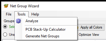
The "Tools" tab has three important functions.
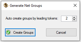
To create net groups, the net names will be used. The number is the number of letters to be tapped. All nets with the same beginning will then be added to the net group. The net groups names depend on the tapped letters.
2. The summary of controls allow you the following operations:
3. The button "Create Group" allows you to create you own groups with the desired group name.
4. This control contains all net groups which are deposited in the ODB dataset. More options to edit net groups can be found by right clicking on a net group.
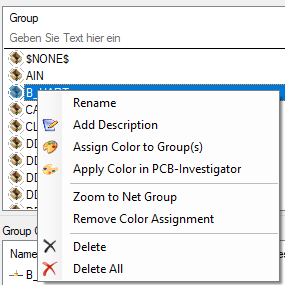
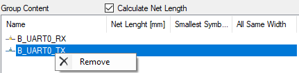
5. Every net of the net group will be shown here, if a group in the group view (4) is selected. To remove a net of the net group, right click the net you want to remove and click remove.
6. If y net group (4) is selected, you can add single nets to the net group with clicking a net in the view with the number 6 and clicking the add button. There are two different add buttons:
For more details have a look to this short video:
By clicking on the Panel Builder symbol, the following dialog will open:
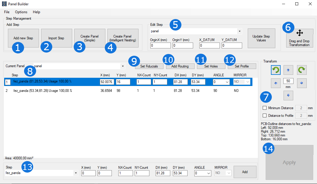
1. Clicking on "Add a new Step" enables you to create an additional step.
2. "Import Step" allows you to import a new design / step from another file.
3. "Create Panel (Simple)" is described separatly and in detail under the post "Create Panel (Simple)".
4. "Create Panel (Intelligent Nesting)" is also explicitly described in an extra post.
5. "Edit Step" is an additional functionality to be used to individually place the origin.
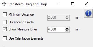
6. The "Drag and Drop" option allows you to manually place the steps on your panel. Clicking on it, the following dialog will open:
7. Clicking on a step in the list, you can transform the selected step by rotating it or moving it in individually set intervals.
8. This list shows all steps currently placed on the relevant panel with its most important information.
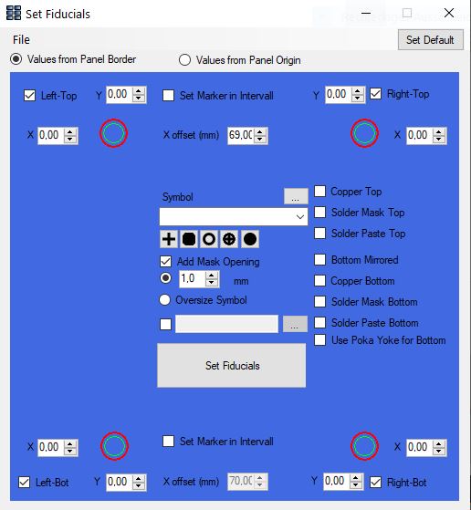
9. Clicking on "Set Fiducials" allows you to define markers on your panel. The following dialog will therefore open:
10. "Add Routing" is used to define the routing for your panel. Clicking on "Add Routing" will open the following dialog:
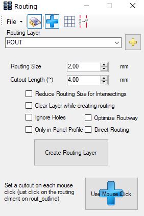
In the File menu you find an extra dialog "cutout editor" see here
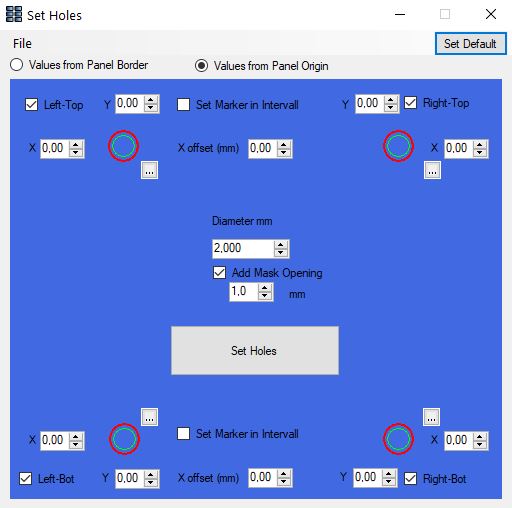
11. For defining holes on your panel, click on "Set Holes". The following dialog will be opened:
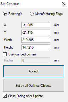
12. "Set Profile" allows you to define the profile of your panel. The following dialog will be opened when clicking on it:
13. Here, you can add another step on your current panel by choosing the step out of the provided list options. You are able to select each step that has been defined for this design.
14. Clicking on "Apply" applies all changes made by you on your currently opened design.
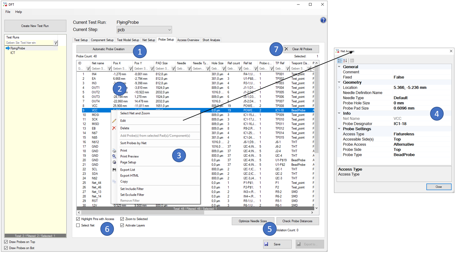
Fixture Parameters:
Tester Type:
Tester Type to use for the automatic probe creation
Probe Side:
Search probes on this/these side(s)
Exclude Single-Pin Net:
Exclude No/Single-Pin Net, all no-pin and single-pin net entries will not create probe entries.
Use max. Test Resources from Net Setup:
If yes, only the given number of Probes are created. If no, all Probes are created
Search Tasks (Top):
Defines the tasks and the order for searching probes on top side
Search Tasks (Bot):
Defines the tasks and the order for searching probes on bot side
Available Needles:
All allowed needles for fixture probes. Will be used beginning with the largest one. Here also the needed distances to components are defined per needle definition
Standard min. Distance to Components:
If no special distance is defined for the given needle, this is the standard min. distance from probe center to surrounding components
Minimum Distance between Probes:
The minimum distance between Probes, measured from outline to outline (taking diameter of the Needle Definition into account)
TP Reference Filter List:
Comma separated reference filter list (e.g. \"TP, P\"). TP Components must start with one of these entries.
TP Pad Recognition:
Recognize test points by the '.test_point' attribute on copper pads.
Minimum pad size to use as probe (Top):
Minimum copper pad size to create a probe for top side.
Minimum pad size to use as probe (Bot):
Minimum copper pad size to create a probe for bot side.
Enable Solder Mask Analysis:
Enable Solder Mask Analysis, only round pads with openings in solder mask are used if this setting is active.
Minimum pad size to use as probe (Top):
Minimum pad size to create a probe for top side.
Minimum pad size to use as probe (Bot):
Minimum pad size to create a probe for bot side.
Maximum drill diameter to use as probe:
Maximum drill diameter to create a via probe.
Enable Solder Mask Analysis:
Enable Solder Mask Analysis, only round pads with openings in solder mask are used if this setting is active.
Minimum pad size to use as probe (Top):
Minimum pad size to create a probe for top side.
Minimum pad size to use as probe (Bot):
Minimum pad size to create a probe for bot side.
Minimum annular ring to use as probe (Top):
Minimum annular ring to create a probe for top side.
Minimum annular ring to use as probe (Bot):
Minimum annular ring to create a probe for bot side.
Fixtureless parameters:
Tester Type:
Tester Type to use for the automatic probe creation
Probe Side:
Search probes on this/these side(s)
Exclude Single-Pin Net:
Exclude No/Single-Pin Net, all no-pin and single-pin net entries will not create probe entries.
Use max. Test Resources from Net Setup:
If yes, only the given number of Probes are created. If no, all Probes are created
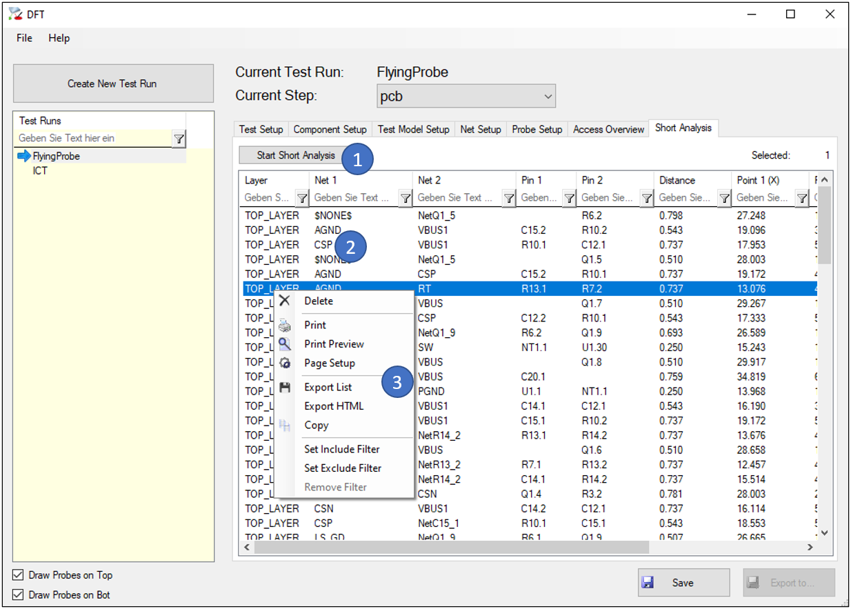
Exposed Copper - Exposed Copper:
The minimum distance between exposed copper areas to not be reported in the Short Analysis (0=deactivated)
Copper - Copper:
The minimum distance between any copper areas to not be reported in the Short Analysis (0=deactivated)
Drill - Drill:
The minimum distance between plated drills to not be reported in the Short Analysis (0=deactivated)
Only Nets with Components:
Only nets with components are checked
Search Tasks (Top):
Defines the tasks and the order for searching probes on top side
Search Tasks (Bot):
Defines the tasks and the order for searching probes on bot side
Minimum distance to Board Outline (Upper Side):
Minimum distance from fixtureless access point center to upper board outline
Minimum distance to Board Outline (Lower Side):
Minimum distance from fixtureless access point center to lower board outline
TP Reference Filter List:
Comma separated reference filter list (e.g. \"TP, P\"). TP Components must start with one of these entries.
TP Pad Recognition:
Recognize test points by the '.test_point' attribute on copper pads.
Minimum pad size to use as probe (Top):
Minimum copper pad size to create a probe for top side.
Minimum pad size to use as probe (Bot):
Minimum copper pad size to create a probe for bot side.
Enable Solder Mask Analysis:
Enable Solder Mask Analysis, only round pads with openings in solder mask are used if this setting is active.
Minimum pad size to use as probe (Top):
Minimum pad size to create a probe for top side.
Minimum pad size to use as probe (Bot):
Minimum pad size to create a probe for bot side.
Maximum drill diameter to use as probe:
Maximum drill diameter to create a via probe.
Enable Solder Mask Analysis:
Enable Solder Mask Analysis, only round pads with openings in solder mask are used if this setting is active.
Minimum pad size to use as probe (Top):
Minimum pad size to create a probe for top side.
Minimum pad size to use as probe (Bot):
Minimum pad size to create a probe for bot side.
Minimum annular ring to use as probe (Top):
Minimum annular ring to create a probe for top side.
Minimum annular ring to use as probe (Bot):
Minimum annular ring to create a probe for bot side.
Offset for the Probe Placement (%):
This parameter is used, if Probes are set to Pins where no TESTPROBE_KEEPOUT but a MPN Package Outline exists. The probe is placed on x % of the distance from the outer edge of the pin to the edge of the MPN Package Outline (also see next parameters). If a keepout is defined, the probe will be placed to the middle of the remaining pin contact area. If no MPN Package Outline is defined, 'Offset Limit for the Probe Placement' is used for the offset.
Offset Limit for the Probe Placement:
This parameter is used, if Probes are set to Pins where no TESTPROBE_KEEPOUT exists. The offset distance calculated with 'Offset for the Probe Placement (%)' is limited to this value, so the offset will not be larger as this value. If no MPN Package Outline exists, this value is used for the offset.
Minimum needed Offset for the Probe Placement:
This parameter is used, if Probes are set to Pins where no TESTPROBE_KEEPOUT but a MPN Package Outline exists. If the offset distance calculated with 'Offset for the Probe Placement (%)' is smaller than this value, no Probe will be placed.
Minimum Pin Size:
Minimum Pin size to be used for the Probe Placement (width and height must be larger/equal
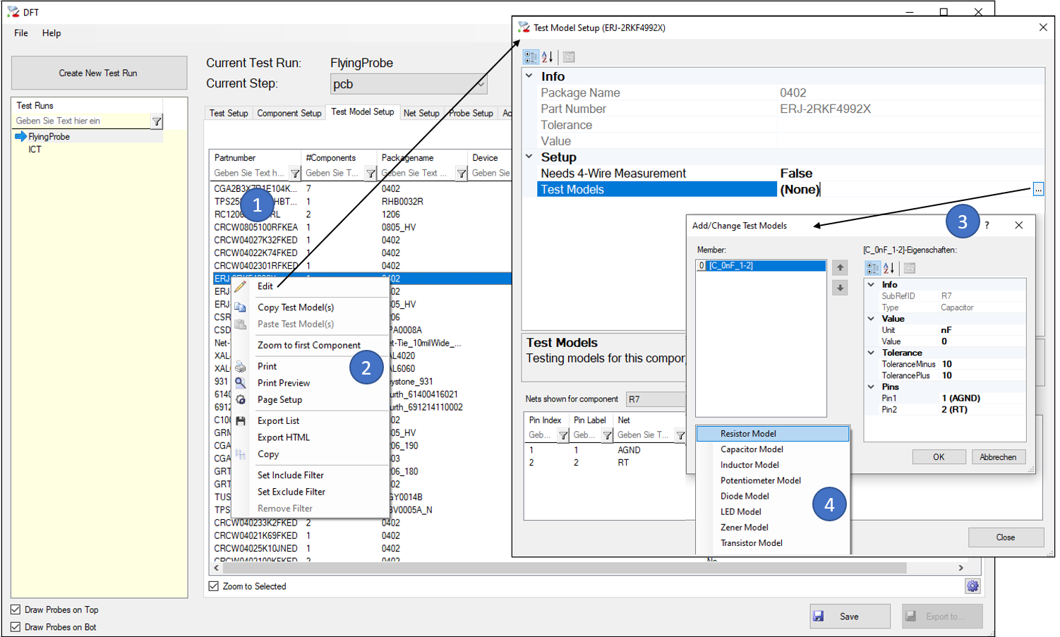
Following test models are available: See appendix.
Additional Rules:
Short measurements will be added in different ways to the exported files:
I3070:
Shorts are not used, as this is a “Fixture” test system
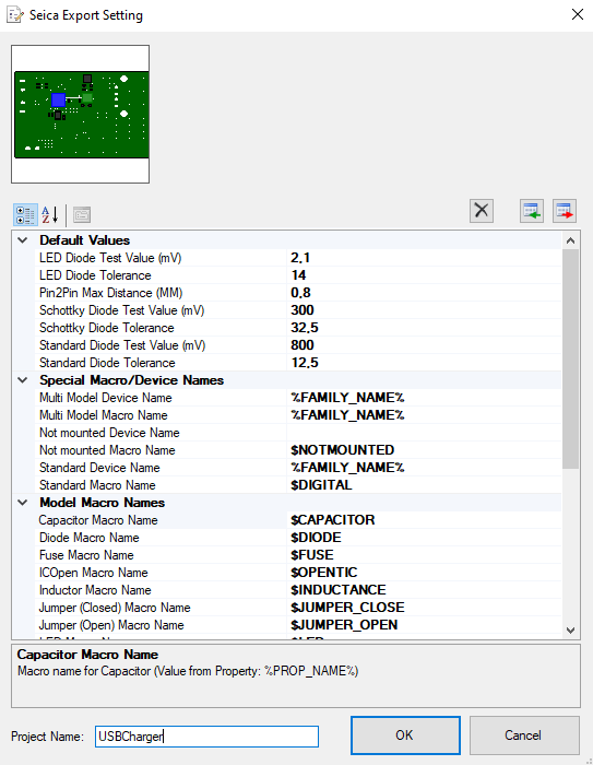
Seica:
Short measurements are exported to the “.shi” file, together with shorts measurements from Pin2Pin test models. Redundancies will be removed first.
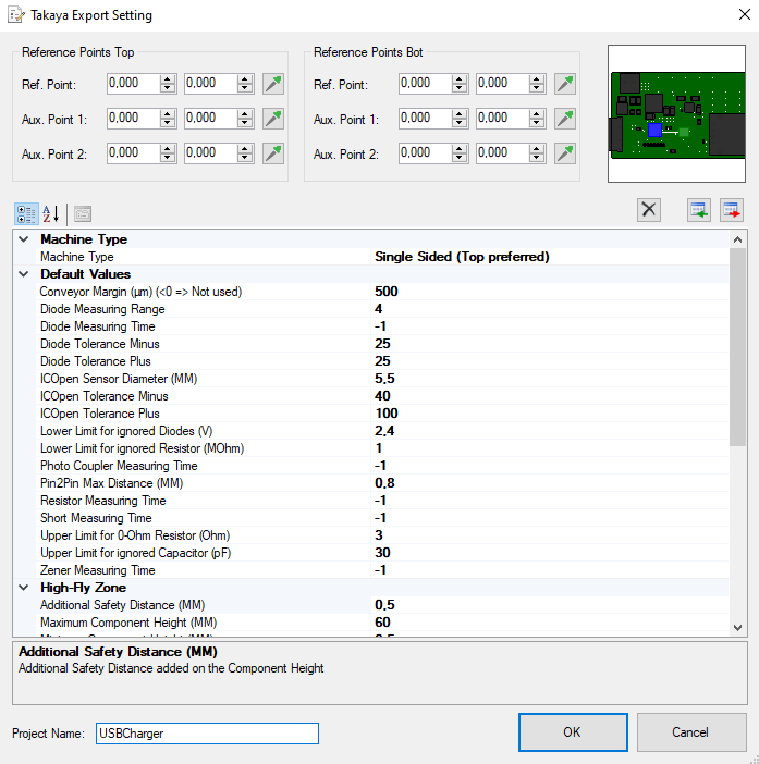
Takaya:
Short measurements are exported as Resistor Tests (@K OP). Redundancies with Pin2Pin test models are removed first.
The Seica export creates a package of files (.alf/.inf/.nod/.par/.sha/.shi) that contain all available component and net information to easily create the test program in the VIVA Software of Seica.
Following export settings are possible:
The Takaya export creates a “.ca9” file containing a whole test program. This includes a wire analysis where parallel and serial Resistors/Capacitors/Inductors are merged if there are not enough probes to test them separately. For small value components, that get lost in the tolerance of the overall circuit, additional Vision Tests are created.
The export can be done for one-sided Takaya machines as well as for two-sided ones (4 fingers on one side, 2 on the other).
Following export settings are possible:
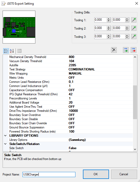
The i3070 export creates a “board” and “board_xy” file that contain all available component and net information to easily create the test program with the native machine software.
Following export settings are possible:
| Model | Parameter | Used for Seica | Used for Takaya | Used for i3070 | Used for Elowerk | Used for Spea |
| Resistor | Type | √ | √ | √ | √ (or OTHER if #Pins <> 2) | √ |
| Value | √ | √ | √ | √ | √ | |
| Tolerance | √ | √ | √ | √ | √ | |
| Pins | × | √ | × | √ | × | |
| Capacitor | Type | √ | √ | √ | √ (or OTHER if #Pins <> 2) | √ |
| Value | √ | √ | √ | √ | √ | |
| Tolerance | √ | √ | √ | √ | √ | |
| Pins | × | √ | × | √ | × | |
| Inductor | Type | √ | √ | √ | √ (or OTHER if #Pins <> 2) | √ |
| Value | √ | √ | √ | √ | √ | |
| Tolerance | √ | √ | √ | √ | √ | |
| Pins | × | √ | × | √ | × | |
| Potentiometer | Type | √ | √ (2xResistor) | √ | √ (2xResistor) | √ |
| Value | × | √ | √ | √ | × | |
| Tolerance | × | √ | √ | √ | × | |
| Pins | × | √ | √ | √ | √ | |
| Diode | Type | √ | √ | √ | √ | √ |
| Diode Type | √ | × | × | × | × | |
| Forward Bias | × | × | √ | √ | × | |
| Test Current | × | × | × | √ | × | |
| Pins | × | √ | √ | √ | √ | |
| LED | Type | √ | √ (as Diode) | √ (as Diode) | √ | √ |
| Color | × | √ (2nd Diode Test) | × | × | × | |
| Forward Bias | × | × | √ | √ | × | |
| Test Current | × | × | × | √ | × | |
| Pins | × | √ | √ | √ | √ | |
| Zener | Type | √ | √ (Zener+Diode) | √ | √ | √ |
| Value | √ | √ | √ | √ | × | |
| Tolerance | √ | √ | √ | √ | × | |
| Test Current | × | × | × | √ | × | |
| Pins | × | √ | √ | √ | √ | |
| Transistor | Type | √ | √ (Transistor + 2xDiode) | √ | √ | √ |
| Transistor Type | √ | √ | √ | √ | √ | |
| Pins | × | √ | √ | √ | √ | |
| FET | Type | √ | √ (FET + Diode) | √ | √ | √ |
| FET Mode/Type | √ (only Type) | √ | √ | √ | √ (only Type) | |
| Pins | × | √ | √ | √ | √ | |
| Fuse | Type | √ | √ (4-Wire if possible) | √ | √ (or OTHER if #Pins <> 2) | √ |
| Pins | × | √ | × | √ | × | |
| Jumper | Type | √ | √ (Resistor) | √ | √ (Switch or Resistor) | √ |
| State | √ | √ | √ | √ (Switch) | × | |
| Pins | × | √ | × | √ | × | |
| Switch | Type | √ | √ (Resistor) | √ | √ | √ |
| State | √ | √ | √ | √ | × | |
| Pins | × | √ | √ | √ | × | |
| PhotoCoupler | Type | √ | √ (PhotoCoupler + Diode + Resistor) | √ (PinLibrary) | √ | √ |
| Pins | × | √ | × | √ | × | |
| Seica: Special Model | DIGITAL | √ | × | × | × | × |
| OPENTIC | √ | × | × | × | × | |
| OPENFIX | √ | × | × | × | × | |
| AUTIC | √ | × | × | × | × | |
| VOLTAGEREGULATOR | √ | × | × | × | × | |
| OPAMP | √ | × | × | × | × | |
| COMPARATOR | √ | × | × | × | × | |
| TRIAC | √ | × | × | × | × | |
| SHORTTEST | √ (in the .shi file) | × | × | × | × | |
| Takaya: Special Model | ICOpen | × | √ | × | × | × |
| Pin2Ground | × | √ (Diode Tests) | × | × | × | |
| Pin2Pin | × | √ (Resistor Tests) | × | × | × | |
| i3070: Special Model | PinLibrary | × | × | √ | × | × |
| Connector | × | × | √ | × | × | |
| Elowerk: Special Model | All Types | × | × | × | √ | × |
| Spea: Special Model | All Types | × | × | × | × | √ |
Exceptional cases:
1. If NO model exists
2. If >1 model exists
3. "Not in BOM" is true
General:
- Comment is set to "NOPOP".
- Values are set to "*".
Special:
- Zener: @K is set to F, @MR can be defined, no Zener Test.
- LED: @K is set to F, @MR can be defined, no color test.
- Transistor: @K is set to JP, no Diode Tests.
- FET: @K is set to JP.
- Switch, Jumper, Fuse: @K is set to OP.
- Resistor, Diode, Pin2Ground, Potentionmeter: @K is set to F, @MR can be defined.
- Capacitor: @K is set to E, @MR can be defined.
- Inductor: Esported as Resistor with @K is set to OP, @MR can be defined.
- PhotoCoupler: @K is set to JP/F(Diode)/OP(Resistor).
- ICOpen: @K is set to JP.
General:
- PartNumber is set to "NOPOP".
Special:
- Resistor is exported as Open Jumper.
- Capacitor is exported with 0.1pF.
- Inductor is exported as Open Jumper.
- Transistor is exported with 0.002/0.001V.
- FET is exported with 99999 Ohm.
- Diode/LED is exported with 0.002/0.001V.
- Zener is exported with 0.001V.
- Fuse is exported as Open Jumper.
- Jumper is exported as Open Jumper.
- Potentiometer is exported with 100MOhm.
- Switch is exported "Off".
General:
- PartNumber is created with export option "Part number field (NOPOP)".
- All test models are ignored and the component is exported as "OTHER".
General:
- In the "Part List" section, the "Mounting Side" is set to "P" (not mounted top) or "M" (not mounted bottom).
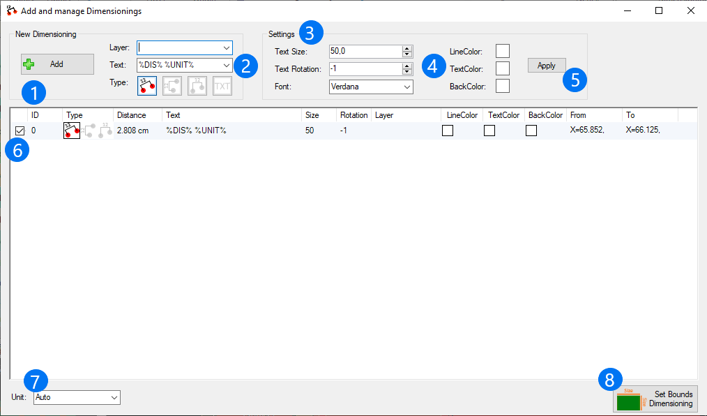
1) After you have adjusted the settings for the next dimensionings you want to add, you can press "Add".
Then, move to the graphic interface to choose two points on your printed circuit board you want to select for measuring their distance. PCB-Investigator thereby helps you with reference points to easily mark e.g. the edge or centre of a component. To set a marker for dimensioning use a right-click. A double-click allows you to change the location of the set marker by entering new values for x and y. You can also easily relocate the connecting line and its associated text information with holding the right mouse botton and shifting the line in its wanted position.
2) Here, you can adjust the settings for the layer, the text and the type of the new dimensioning you want to add.
3) There are three more options you can adjust before adding a new dimensioning: text size, text rotation and font.
4) You can also determine the colors that should be used for the visualization of the dimensioning: line color, text color, back color.
5) Clicking on "Apply" allows you to subsequently change the settings of (3) and (4) for all dimensionings you have determined so far at once.
6) In this list, you will find a overview of all dimensionings you have determined with all their relevant information. You can also adjust the settings by double-clicking on the intended configuration. A right-click on a dimensioning will highlight the appropriate dimensioning in the graphic interface.
7) Here, you can choose the unit you want to use for your dimensionings. Selecting "auto" will apply an automatically choosen unit (most practical solution) for each dimensioning. To avoid misunderstandings using "auto", you should indicate the unit for each of your dimensionings (2).
8) "Set Bounds Dimensionings" sets the dimensionings for your overall printed circuit board (lenght, width).
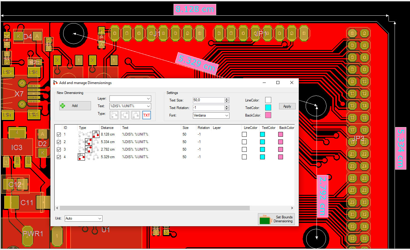
Example for dimensionings on a design:
View Dimensionings:
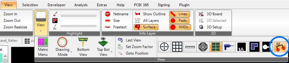
To display or hide your dimensionings, click on the framed symbol which can be found under "View".
To import components, you can use the Component (CSV) Import.
This works for all excel or CSV files with References and X/Y positions. If you have only BOM Information you have to use the Part Matcher

The import is easy to use, PCB-Investigator will try to find the columns but user can modify the table indizes manually.
The settings gives you options to identify the packages and place new components with different methodes:

1) options depending to the import table e.g. the unit of X/Y coordinates or the rotation direction (clockwise or counterclockwise).
2) Use existing libraries e.g. the easylogix shared EPackLib to find package outlines and optional part information (with option to set missing packages by part outlines).
3) Package Finder gives many options how to identify the packages, with "Check for Similar Package Names" small nameing differences e.g. 0603C and 0603_C handled identically. Most Important for exising footprint layer is the compare of package footprint with existing pads.

In the Results tab you have some more options:
1) Check each placed package in the Result list, there are markings for Missing/Created and Updated packages
2) Compare with the library, the founded result list (Alternative packages with score) and directly compare all placings in the design
3) Edit the result or replace missing dummy packages with different libraries. You can also create new packages via pad selection with "Create Package from Selection"
Here a short video with the complete workflow:
To view the BOM, use the Component Manager (see Working With Components or here).
To export and print the BOM, use the "Export" tab.

If you want to transfer the components to an other design, you can use the Component List Export and on the other side the CSV Import (see above). But this is only working if you store your package/part definition in an library.
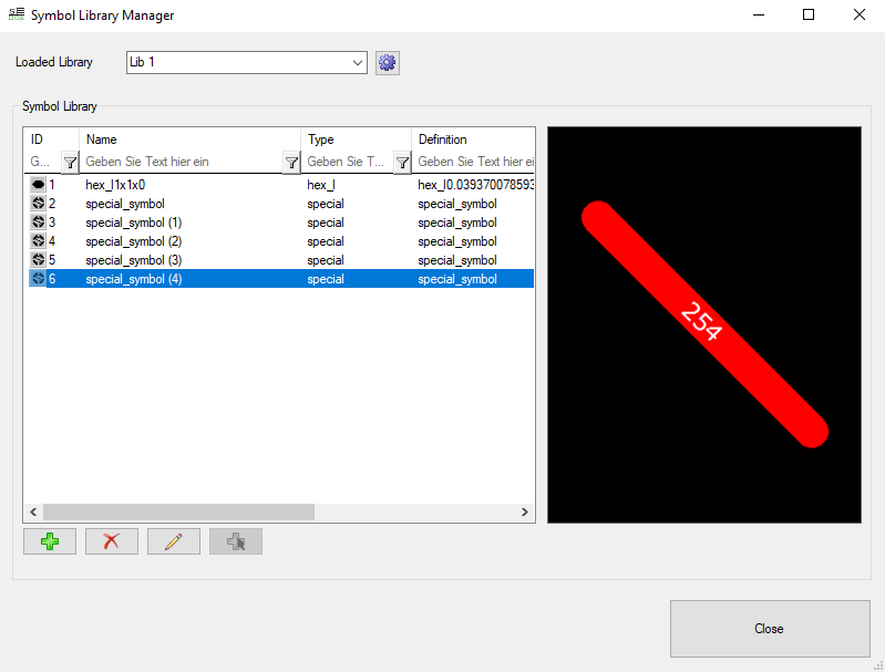
Symbols / Objects are stored in the symbol library. You can either access it when e.g. adding or editing objects or you can directly open the symbol library.
By clicking on the tab “Symbol Library” which can be found under the ribbon “Fabrication”, the following window will open.
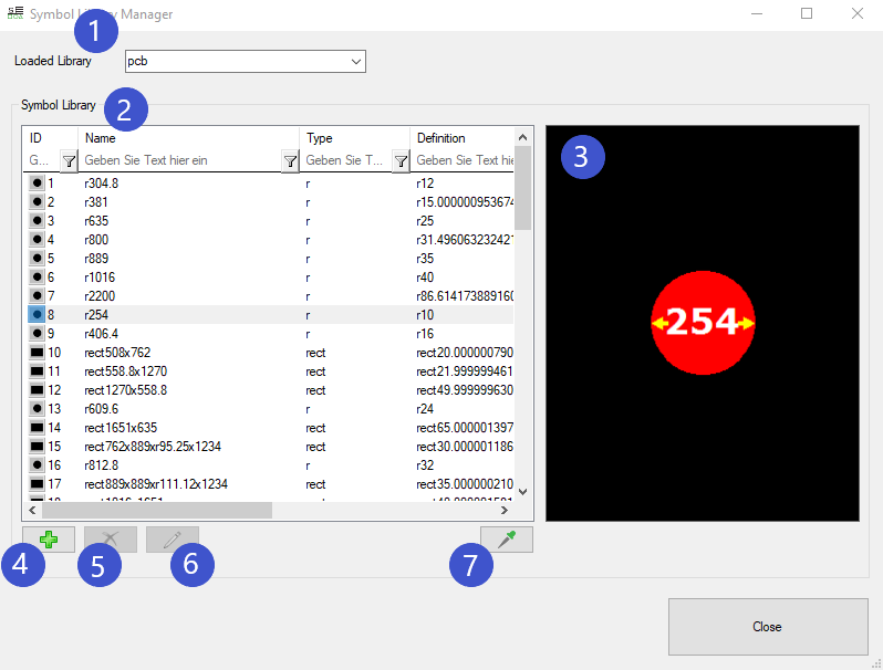
1. Under “Loaded Library”, you have three different types of libraries to choose from:
To get access to the symbols of one of these symbols, you have to open the subcategories of the corresponding library.
2. Then, you will see a list with all symbols and their properties stored in this library.
3. Selecting one of these symbols in the list, will visualize them on the right side of the list.
4. Clicking on the green plus at the bottom left corner of the dialog will open the following dialog:
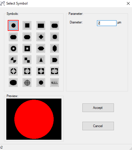
Here, you have the choice between different ODB++ symbols that can be adjusted according to your needs by defining their parameters. Clicking on “Accept” will then add the newly defined symbol to the currently opened Library.
5. Clicking the “X” when you have selected a list item, allows you to extinguish this symbol in your library.
6. Clicking on the pen symbol will open up the “Symbol Property Editor”.
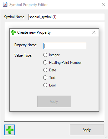
The Symbol Property Editor allows you to change the name of the symbol and create a new property by entering a new property name and by choosing a new value type for the symbol.
You can´t delete or edit the properties of a symbol that is a regular feature of your design. When you have selected one of these symbols, the two buttons will be greyed out.
7. If you have selected the currently opened Job as a Library, you have the option to pick any of the symbols on your design in the graphic interface and the corresponding symbol in the list will be highlighted.
There are two more options when you have selected an XML or 365 Library to work with. The dialog for these libraries will also look a bit different:
When choosing either an XML or PCB-I 365 library, you can click on ![]() to open another dialog for adjusting the settings of the library.
to open another dialog for adjusting the settings of the library.
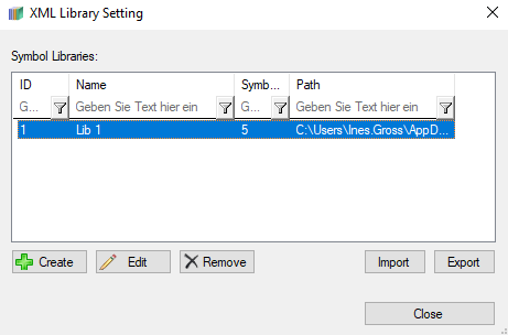
This editor allows you to create, edit, remove, import and export a (new) library. When adding a new library (click on “Create”), you have to enter a new name for the library and you have to select the propriate path for the library file you want to choose.
If you want to remove a symbol library in the setting dialog by selecting it and clicking on “Remove”.
You can also edit the parameters of an already existing object or add a new symbol from the current selection. Clicking on ![]() or double-clicking on a symbol in the list will open a new window of PCB-Investigator allowing you to adjust the currently selected symbol in the list to gain a special symbol that’s not contained in any of the libraries.
or double-clicking on a symbol in the list will open a new window of PCB-Investigator allowing you to adjust the currently selected symbol in the list to gain a special symbol that’s not contained in any of the libraries.
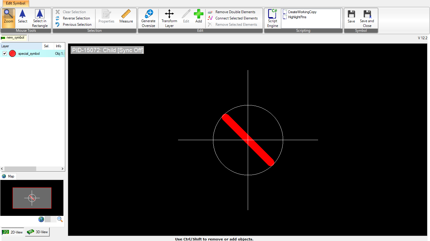
To configure this symbol, you can then click on “Add”. This allows you to compile a special symbol. How to add symbols or objects is described under “Add Objects”. If you have completed the compilation of your special symbol, you can click on “Save” or “Save and Close” on the upper right corner of the window and you will get back to the main Symbol Library dialog.
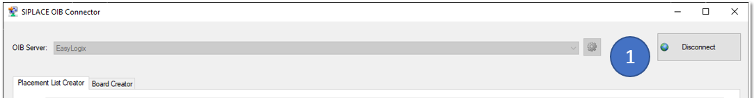
When you open the "SIPLACE OIB Connector" (in the 'Machine Export' menu) the first time, you have to first enter your OIB server settings by clicking on the gear button (1):
Following dialog will open:
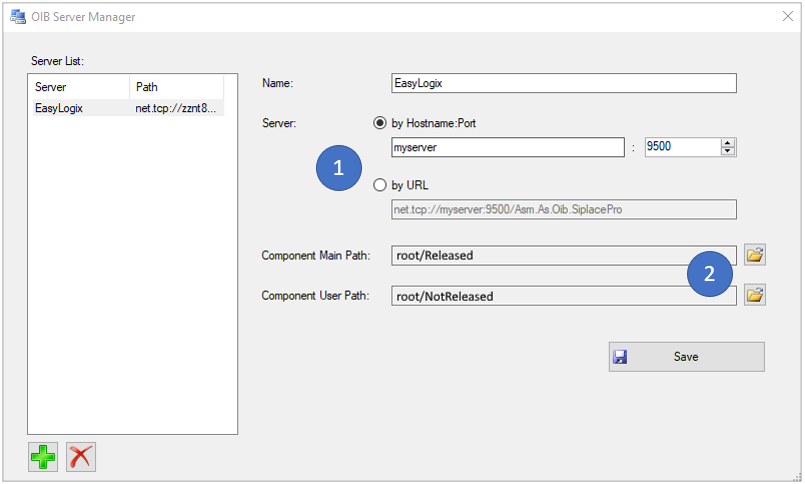
In this server manager, you can organize multiple OIB servers. To create a new one, please press on the little green "+" button and enter a name.
Afterwards you'll have to specify the OIB server adress by entering an IP/Hostname + Port, or directly enter the 'net.tcp://...' adress (1).
When this is done, you'll have to specify two server directories by clicking on the small browse button (2):
Click "Save" and close the dialog to preceeed.
To start, please select a server and click "Connect" (1).
With the "Placement List Creator" tab, you can create placement list elements for each component side on the OIB server.
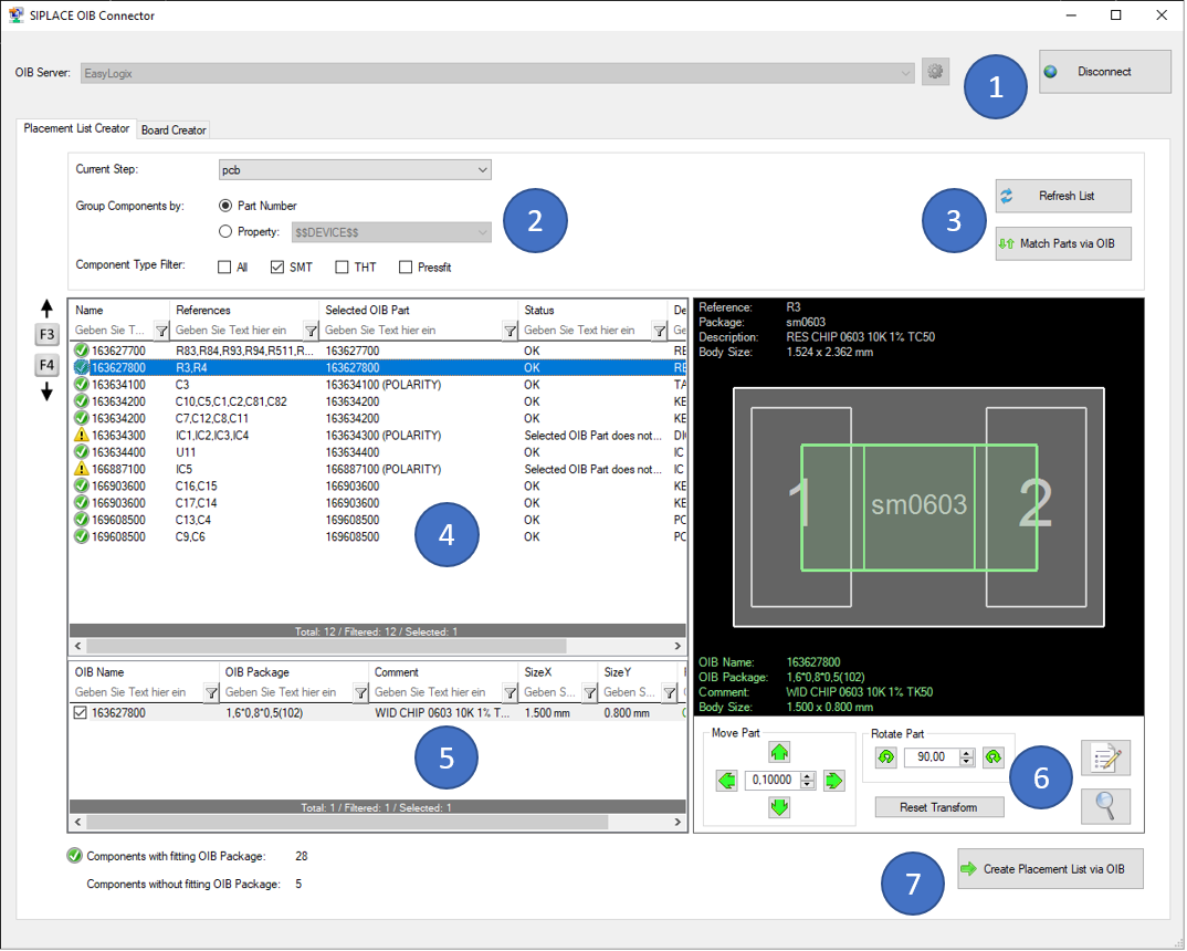
To start, you have to do a few settings in block (2):
Always when you change settings in (2), you will have to 'Refresh' the list and 'Match Parts via OIB' again (3).
When the matching process is done, you will see all your filtered parts in the list (4), including an overlay of the matching OIB part definition on the selected server. Found OIB parts are centered on the CAD package center. Details of the found OIB part and the fitting state are listed on the bottom side (5).
The 'Status' column indicates, whether a OIB part was found or not, and if the found part fits onto the CAD package. The condition for fitting is, that the pin definition of the OIB part must at least partly overlap the CAD package pin.
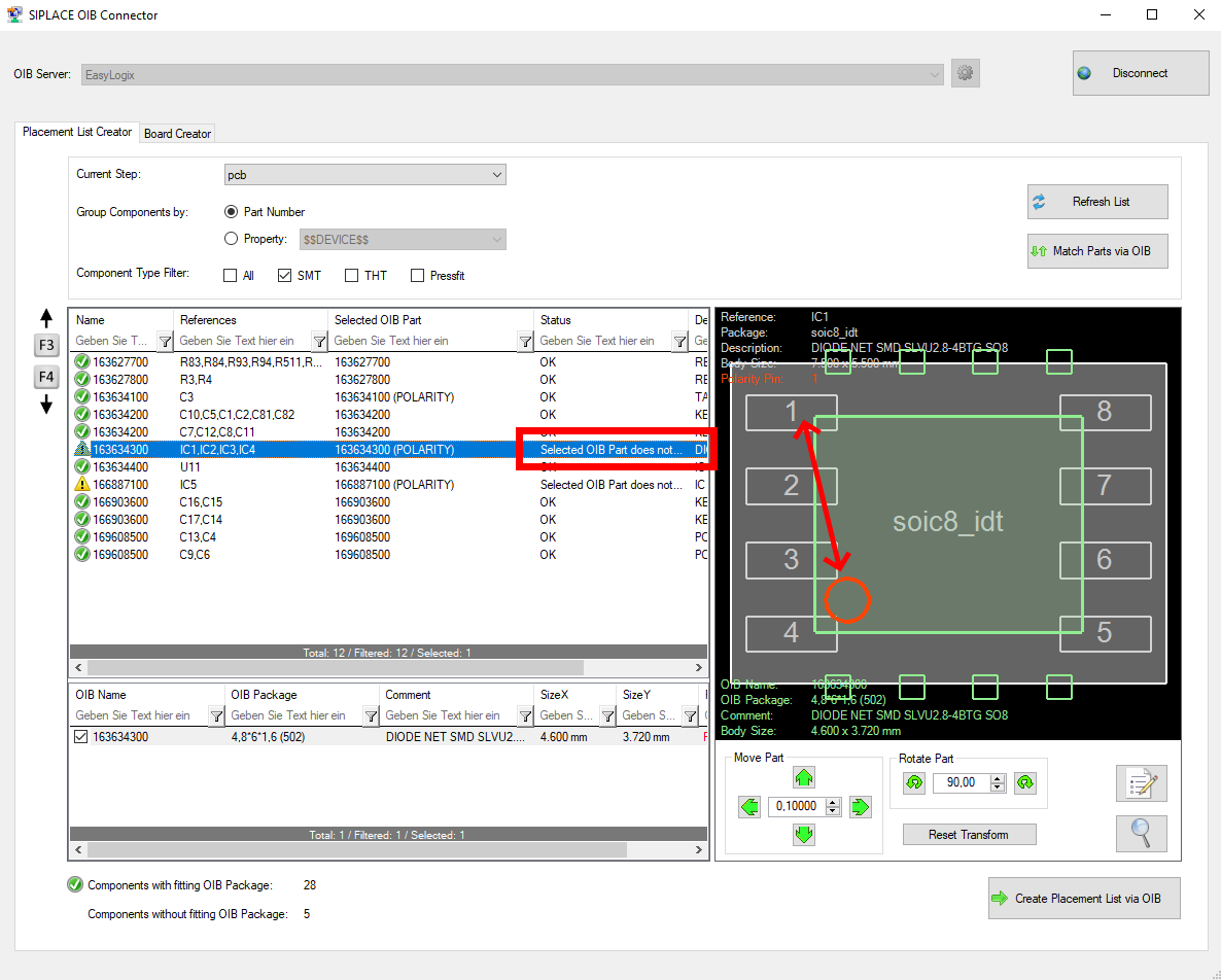
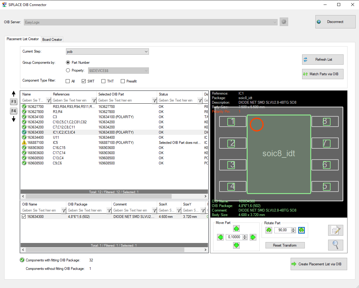
If the found part does not fit, you have the possibility to shift its position or to rotate it until it fits (6). With the two buttons in this block on the right, you can open the property dialog of the CAD component or zoom to it.
If the OIB part has a polarity definition, this polarity marker is visualized in red. The fitting alorithm then also uses the polarity information, to recognize if the component is correctly rotated (CAD polarity pin is same as OIB polarity pin).
Example of the fitting process (6) (by rotating 90° clockwise):
 =>
=> 
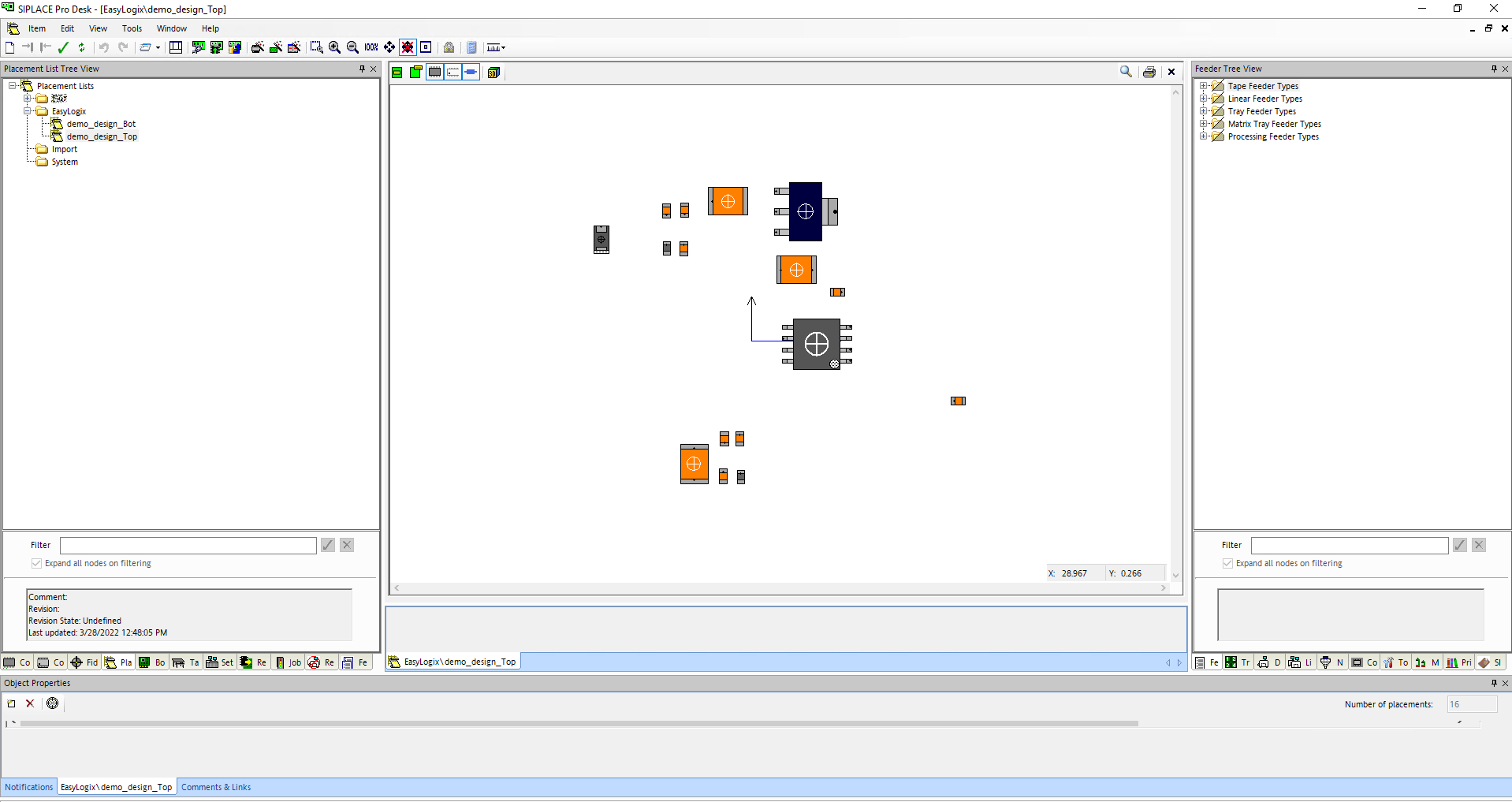
When clicking the 'Create Placement List via OIB' button (7), you are asked to select a folder on the OIB server and enter the name for the placement list(s) for top and/or bottom side. Afterwards, the placement lists are created via OIB. Missing parts, that where not found during the matching process, are automatically created in the 'Component User Path' (see 'OIB Server Manager'). Those created parts are dummy parts without any real outlines or pin definitions. Their information must be completed by the user in the SIPLACE Software afterwards. Components that have the ".comp_ignore" attribute are marked as 'omitted' in the placement list.
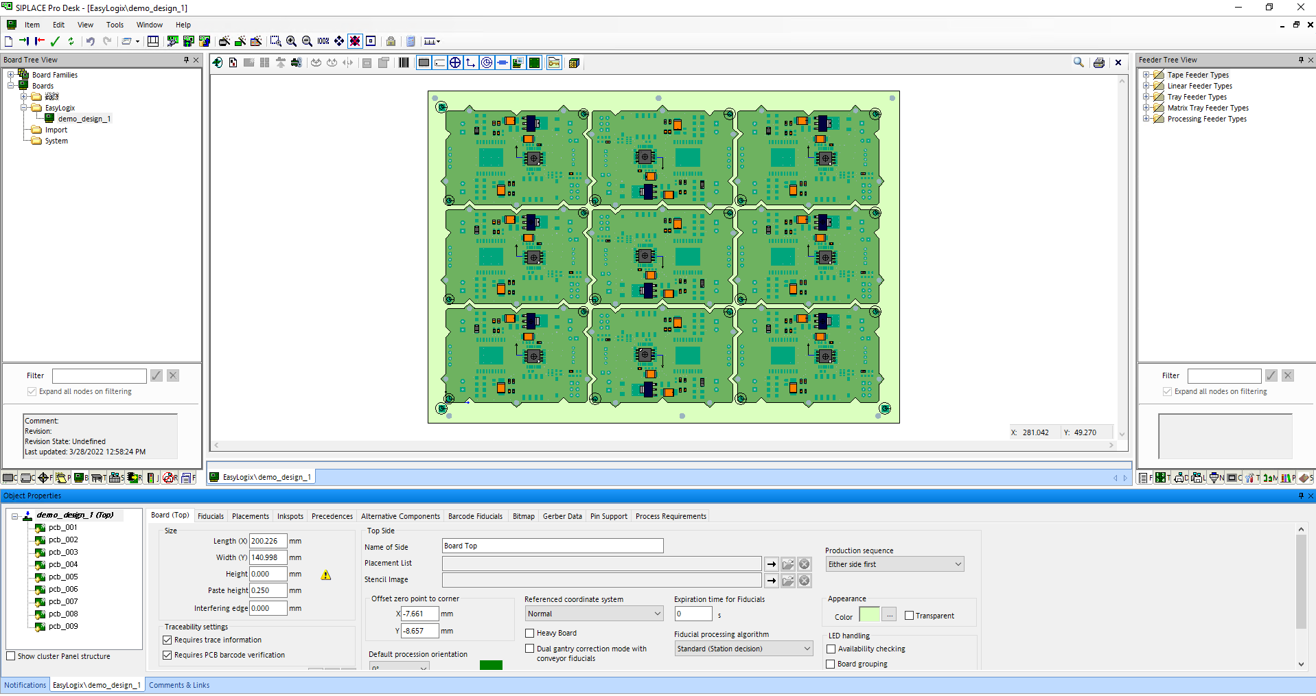
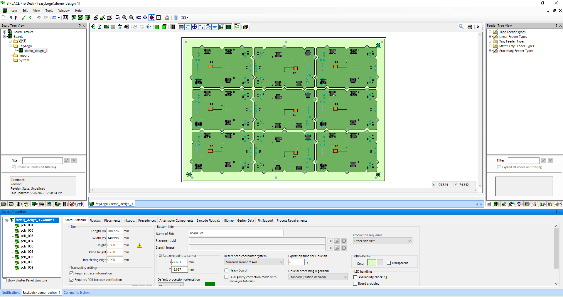
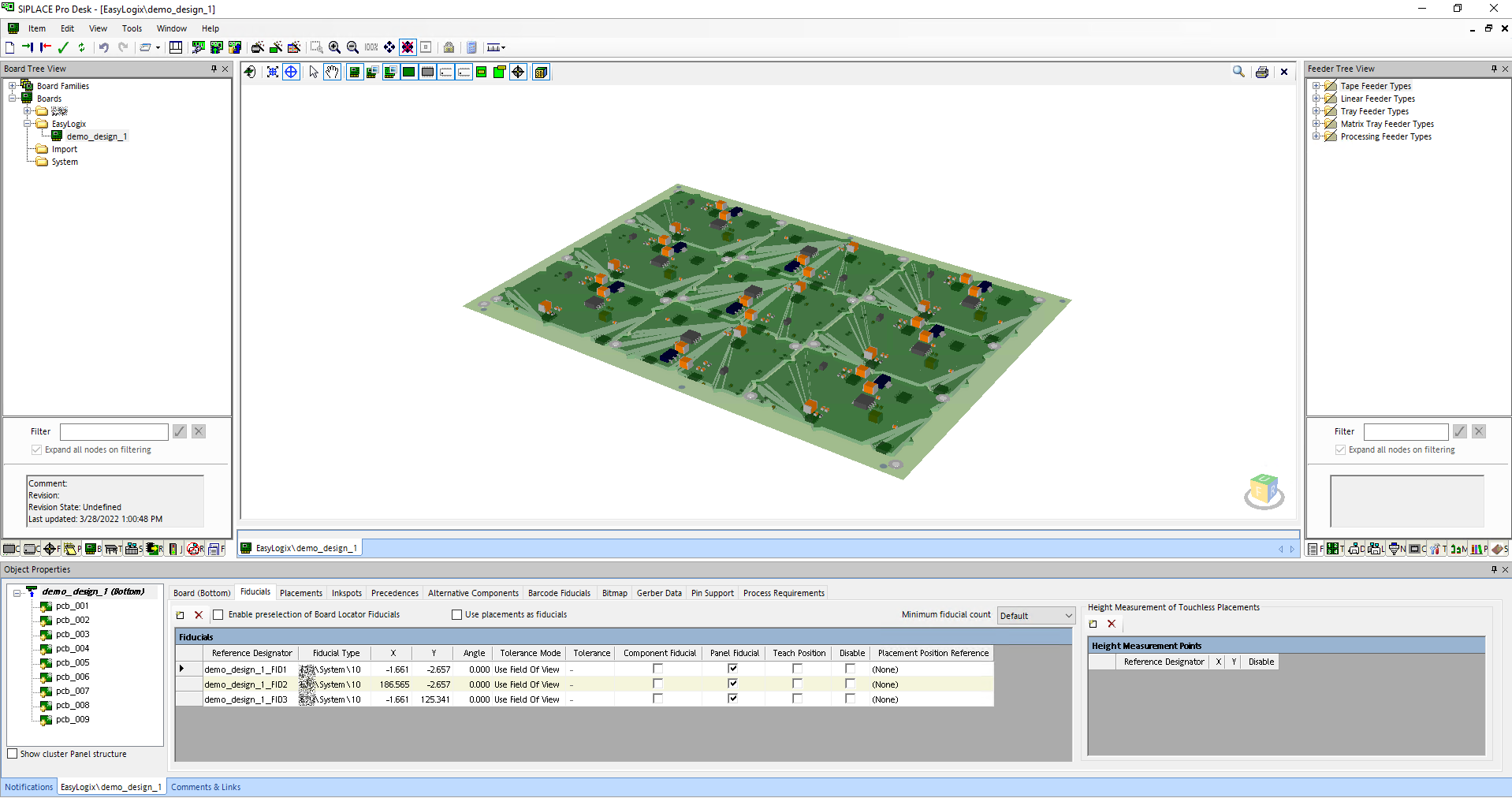
Here is a screenshot of the result in the SIPLACE Software:
After having created the placement list of the single board(s), you can create the panel data with the "Board Creator" tab.
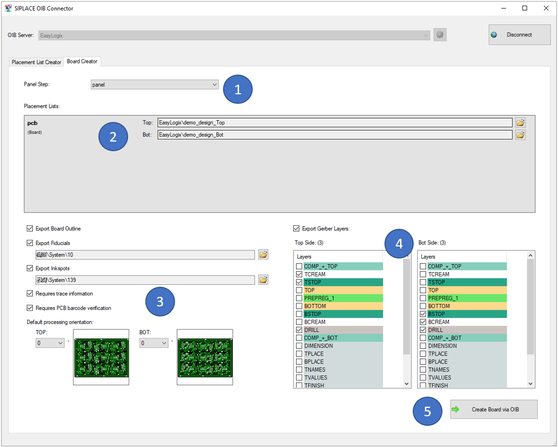
To start, you have to select the panel step that should be created (1). It is also possible to create panels in panels (recursive), when the most outer panel is selected.
For the given panel, the included single board(s) is/are listed unter (2). Here an already existing placement list on the OIB server must be selected per board and side. If the placement lists where created before in this session with the "Placement List Creator", the information is already prefilled. If not, you can click the small browse button and select the right placement list.
In the block (3), there are different options available:
In the block (4), you can choose which CAD layers should be exported and imported in OIB for this board per side. It is mainly thought for paste/mask layers.
When clicking the 'Create Board via OIB' button (5), you are asked to select a folder on the OIB server and enter the name for the board entry. Afterwards, the board is created via OIB.
Here is a screenshot of the result in the SIPLACE Software:
With the "SIPLACE QD Exporter" tool, you can create '.qd' files including placement lists and board information for ASM machines.
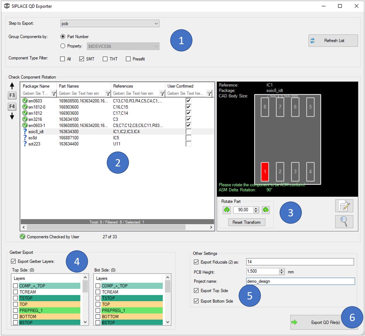
To start, you have to do a few settings in block (1):
Always when you change settings in (1), you will have to click at 'Refresh' to update the list. In the list (2), you will see all packages and the corresponding parts for each step or sub-step of your selected (panel) step.
It is then important so select list entry by list entry to check the rotation correction. If a entry is selected, you'll see the package drawing on the right side. You have to rotate this package to be displayed in exactly the same way, as it is defined on the ASM machine ('make it ASM conform'). You can confirm this by checking the "User Confirmed" checkbox in the list's last column. The rotation can be done by using the buttons in (3). Here, the rotation can also be reset and with the two buttons in this block on the right, you can open the property dialog of the CAD component or zoom to it.
In the block (4), you can choose which CAD layers should be exported as gerber files next to the '.qd' file. These gerbers can then be also imported in SIPLACE. The mirroring/translation of the bottom gerber is already done in the gerber itself, so that you do not need to transform the layers in SIPLACE.
In the block (5), there are different options available:
When clicking the 'Export QD File(s)' button (6), you are asked to select a folder where the files are exported to.
Here are some screenshots of the result in the SIPLACE Software:
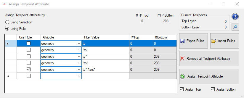
You can find the Testpoint Assign Tool under Plugin >> Assign Testpoint Attribute.
This tool helps to find and mark testpoints in a layout which could be defined via multiple non standardized attributes. Marking them with this tool then helps to standardize this and prepare the layout for following tools (for example the DFT Preperation).
On the top left you can switch between using the current selection or a set rule to find the testpoints and assign the test_point value.
When choosing rules you can add another rule by checking the checkbox of the lowest row in the current listview and then fill out which attribute should be tested and what value needs to be set in said attribute.
All attributes are listed in a simple drop down menu. The Filter Value then has to represent the value of the attribute. Wildcards are allowed when searching for attribute values. The image shows for example all ways to search for "tp" in the "geometry" attribute:
Also it is possible to search for multiple values of the same attribute as shown in the last row. Simply seperate the values with a semicolon.
Boolean attributes do not need any value since their existance already means they are set.
To remove a rule simply select the whole row by clicking on the left most column of the row you want to delete (left of Use Rule) and press the "delete" key on your keyboard.
Checking a rule will select all found possible testpoints of the job (the checkboxes Assign Top and Assign Bottom change the selection depending on the check state of them)
On the top right side there is an information panel showing:
Export Rules exports the currently set rules to a xml file on selected location on the machine or in a cloud
Import Rules imports rules from a file either from the machine or from a cloud
Remove all Testpoint Attributes removes the "test_point" attribute from all pads of the job
Assign Testpoint Attribute adds the "test_point" attribute to either the currently selected pads or the pads found by the selected rule (handled by the radiobuttons "using Selction" and "using Rule")
Assign Top is a checkbox that when unchecked the "test_point" attribute will not be set for the pads on the top layer
Assign Bottom is a checkbox that when unchecked the "test_point" attribute will not be set for the pads on the bottom layer
To find possible testpoints the attribute histogram is a good way to start.
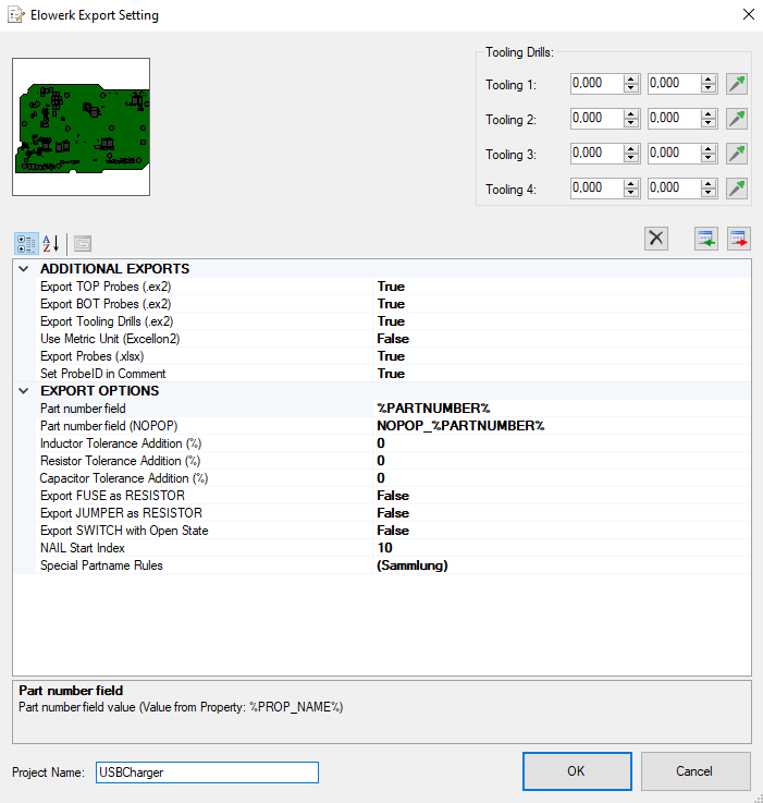
The Elowerk export creates a “xCAM” file that contain all available component and net information to easily create the test program with the native machine software. Optionally also Excellon2 files to create the adapter can be exported.
Following export settings are possible:
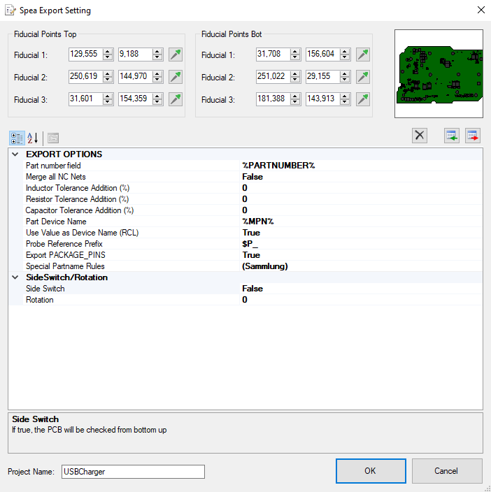
The Spea export creates a “CAD” file that contain all available component and net information to easily create the test program with the native machine software.
Following export settings are possible:
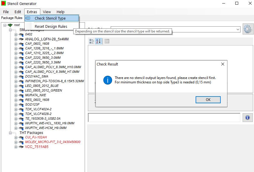
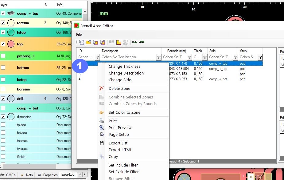
The Stencil Generator uses all zones defined by the Stencil Area Editor. If there are no zones the outline will be used as main zone. Use default rules for your company. Setting a package group, enables the Wizard to set the rules regarding it. SOICs, Chips, BGAs and any definition needed. The Wizard is delivered with predefined settings. To adjust all data preparation to your product you can setup own data preparation Scripts to adjust to your equipment.
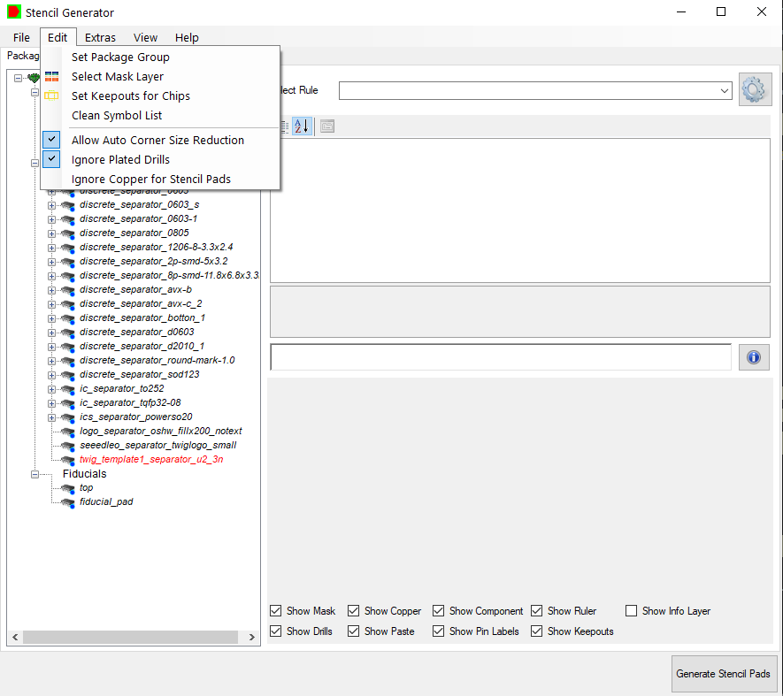
Set Package Group is only necessary if your data don’t contain a proper information. Customers with EPL (“Easylogix Part Library”) can resolve trusted data from EPL. The Wizard also process layouts with multiple mask layers in the stack-up. Set “Keepouts for Chips” is only available if you have MPN packaged defined. It will handle the usable area for you. You also can set plugged drills as free usable area.
You have the possibility to set rules by package, set extra rules for components in defines zones or to set a rule for each component.
To set another rule to your component, select one in the given list.
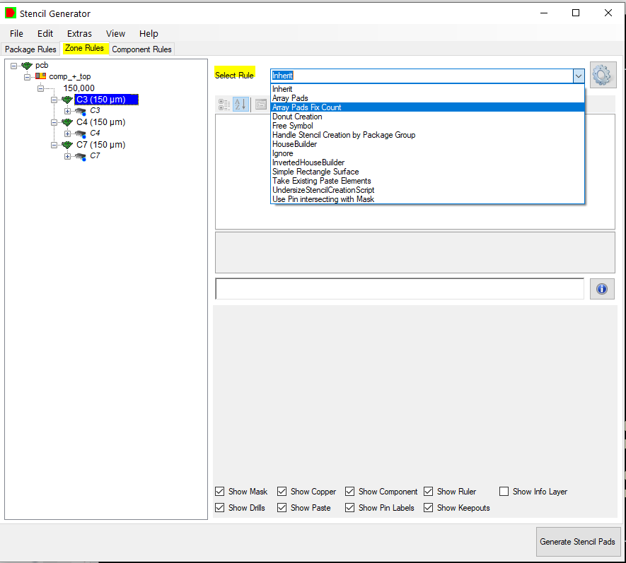
You can add your own rules by clicking on the setting symbol.
Send the stencil data in your preferred format to your supplier |
Result of the rule-base stencil wizard |
Before and after |
Stencil pad details |
Here is a short video to show special cases in one of our demo designs:
Note: For high quality, it is recommended not to cut pin pads. You can combine areas e.g. from different parts to get ideal areas.
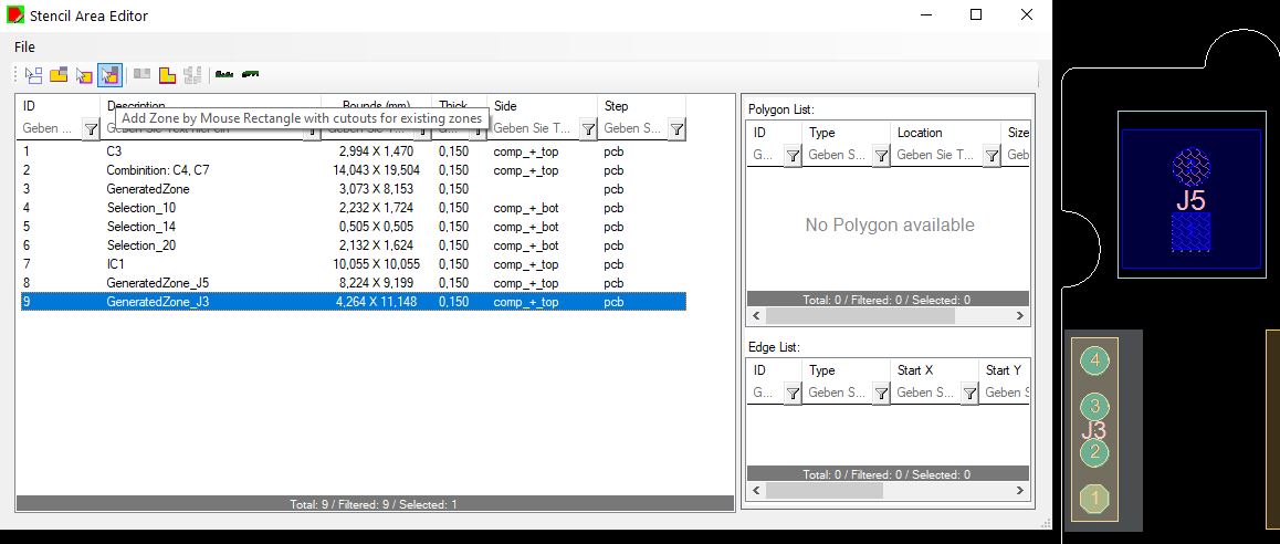
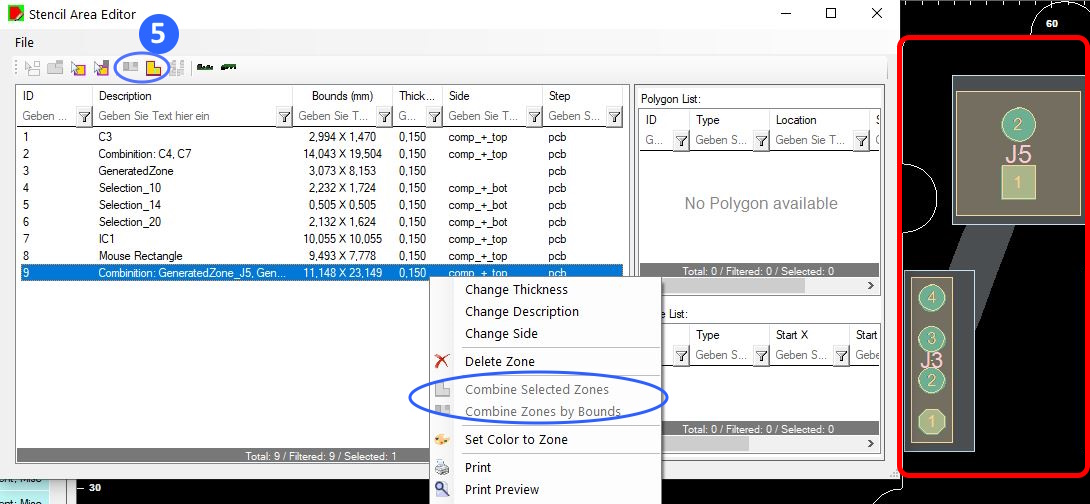 Combine different zones to one zone
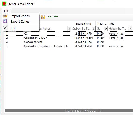
-->Zone settings can be saved in ODB attributes, exported as xml and imported from xml.
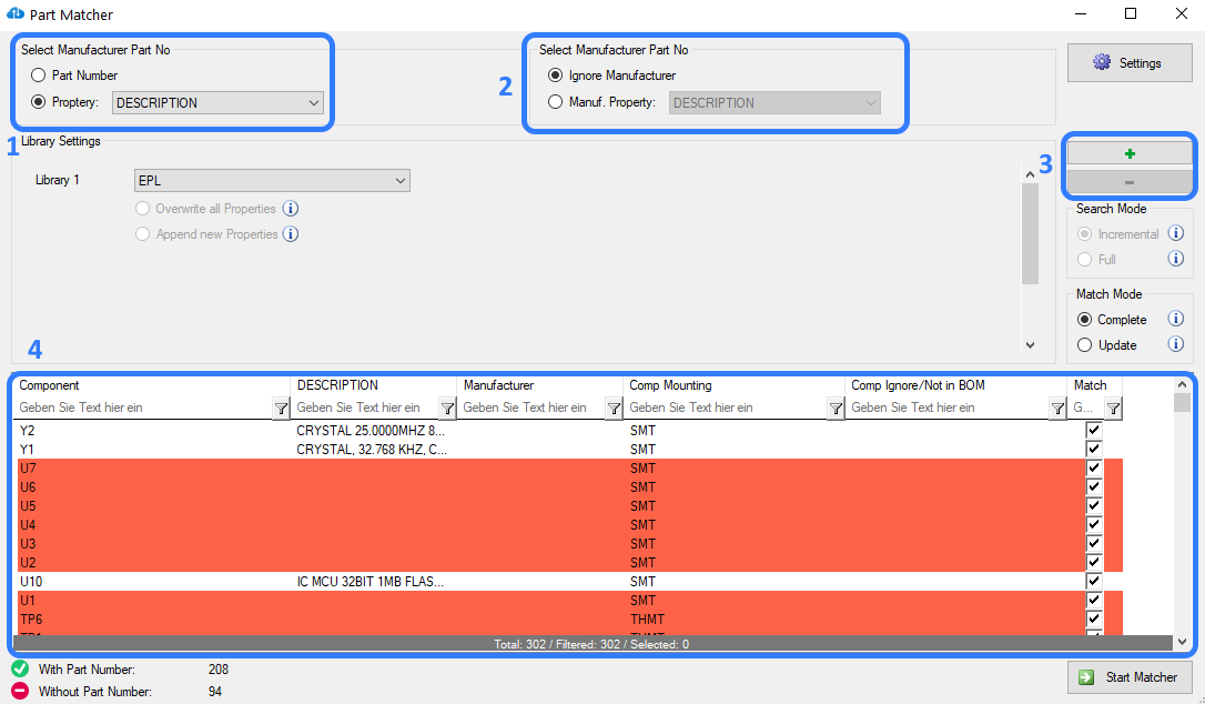
1. Select Manufacturer Part No: You can choose between "Part Number", which shows a fixed attribute of the part, or "Property", where you can select any property which contains the value for the MPN. This setting is used to match parts in the selected libraries.
2. Select Manufacturer Part No: Additionally, the manufacturer can (but does not have to) be included in the search (selection of an attribute of the component in which the manufacturer is located). This setting is used to match parts in the selected libraries.
"+" -add new library "-" -delete last library to search
4. Components List of all components in the current design with selected values for Manufacturer Part Number and Manufacturer. Highlighted components does not have values for the selected Manufacturer Part Number and Manufacturer property and can not be searched by the Part Matcher. The checkbox can be used to select the components which should be matched by the Part Matcher.
User Credentials to log in or change user
The Production Tool Editor to define solder frames:

The solder frame definition based on an single PCB with fixing elements as well as down holder with routings for spcial cases like THT components.
The Production Tool Editor to define coating carrier:

The coating carrier base on an standard frame (or special format) with down holder, fixing elements and many more. You can individually change the coating machines to create coating areas and check the frame use legal regions for coating. For better support in the frame you have options to use different routings and depending on the extra material it automatically creates the openings for the coating machine heads.
The Production Tool Editor to define workpiece carrier:

Workpiece carrier containing extra elements and routings, this simple frame create an simple transporting frame with down holders to fix the PCB in the production process.
The Production Tool Editor to define supporting plates:

Supporting plates for pressfit actions in your production line do create routings and documentations for the export files.
The Production Tool Editor to define adapter definitions:

The adapter definition is the most complexe production tool, it contains all standard cases for special testing routines e.g. high voltage checks or vacuum systems. Special handling for connectors, LED Checks, switches or press buttons included.
You can handle stops and fixing elements as well as routings for high components and down holder or supporting stamps. After defining all important elements it is possible to add an example adapter panel to export the adapter package for one DFT Session.
The export contains additional files to create 3D modells like this:

(3D view contains PCB, models for fixing pins, extra electronic and the adapter case)
Watch our PCB-Investigator - DFT Preperation Video here:
Tutorial: DFT Preperation & Machine Export:
The Cutout Editor helps you to create additional elmenets and modify the cutouts:

1) List of all cutouts, they have an running ID and a Location X/Y for special cutouts there is also and End X/Y and an repeat Index (for each child step).
2) Edit area for the cutouts, you can modify the Location.
3) Additional Element Area, here you can define what you need on different layers
4) Auxilary Drills is special, you can generate mousebites for one or both sides.
For setting mouse bite drills we have a second video:
The Package Library Manager handle all libraries for packages, this could be e.g. an 365 library, an lite DB or an xml library and customized libraries:

You can edit the packages here and change properties.
Here is a short video to show how you can add your own library:
The part library manager gives you options to edit your list of part libraries:

With some options to copy/delete/add new parts you can manage your libraries here and manage the available libraries in the settings dialog:

The library types containing data from the open Job/Design, local types like xml or lite DB and online types like API Part Libraries, REST Libraries and out 365 Libraries:

With the context menu you have options to copy or edit the part, you can export the library list and search for specific information:

Here is an short video how to bring parts in your library:
use the pencil button to edit package properties in an seperate dialog:

Depending on the library type there are different properties available, with 365 libraries you can manage your properties in admin area or in xml library you can directly change the available properties.
use the pencil button to edit part properties in an seperate dialog:
Depending on the library type there are different properties available, with 365 libraries you can manage your properties in admin area or in xml library you can directly change the available properties.
All Nets can have net attributes, if you set an Net Group it will be handled in some plugins together.
To find out how you can set this net groups read this page

There are some basic settings to match the packages.
Pin Positions are always used, but you can change the Height information of your CAD Data to tolerance value based on the component height or ignore it complete.
Overwrite package and step information defaul by "Ask", this mean there comes a dialog with checkboxes.
How to use the Package Expert firt time?
Here is a short video how to ask Library for all components and set 3D settings:
Connect Library information with your AVL File, with individual importer it can read csv, excel and other files.
Check all components with vidual fitting helper and maybe transform wrong locations or rotations with the simple user interface:

Depending on the MPN and Manufacturer the BOM Expert search for library information and connect them with the open design, this can include properties and step files. You can automatically set no_pop/comp_ignore attributes and use custom actions with an post script to do special actions depending on the imported data.
The Settings containing a list of importers, Searchend Properties and settings to handle not found components. It also has options to add missing entries in an intermediate library and an post script (found by GUID in your favorites).

Unknown => It is not possible to give more details
ReferenceNotInDesign => The reference in imported data is not available in the design
ReferenceNotInAVL => The component in the design has no entry in imported file
NoPartAvailable => The part list do not contain results in the selected library
NoPartSelected => No part selected mean the user has to select one
NotFoundInLib => The library do not contain a fitting item
SelectedPartDoesNotMatch => There is a maybe wrong part selected, please check the selected part
OK => Part is OK
OKUnverified => The pin matiching is not checked but the part is marked as OK
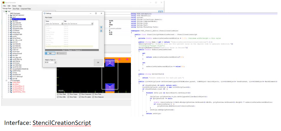
To automate your custom stencil scripts, it is necessary to use the StencilCreationScript interface.
Here is a link to see all details for your implemention manual.
You have to set public porperties to give user options to change in the property grid, there is also a method to create the preview and the pads. You should fill the corde with all calculation you need e.g.
public bool CreatePads(IPCBIWindow parent, IStep step, IODBLayer StencilLayerOutput, InterfaceCMPObject BasicObjects, List<IPolyClass> UsedPinPads, List<IPolyClass> MaskForCheck, List<IPolyClass> Drills, double ThicknessPaste)
{
if (StencilLayerOutput == null || BasicObjects == null || UsedPinPads.Count == 0)
return false;
bool IntersectWithMask = false;
CreateRectangleElement(StencilLayerOutput, UsedPinPads, MaskForCheck, Drills, BasicObjects, out IntersectWithMask);
return true;
}

In the options area (1) you can add your custom developed scripts (2).
In stencil design, a donut shape is used to define a circular opening with a central void (hole), commonly used for thermal reliefs or annular ring designs. The donut is generated around a pad center based on several configurable parameters.
| Property | Type | Description |
|---|---|---|
InnerDiameter |
double | Defines the inner diameter of the donut. This is the size of the central hole that will not be cut into the stencil. |
OuterDiameter |
double | Specifies the outer diameter of the donut, representing the total size of the stencil opening. |
AngleStep |
double | Angle between each arc segment when constructing the donut shape. A smaller step creates a smoother circle. |
OffsetX |
double | Offset in X-direction from the pad center, applied to reposition the donut shape. |
OffsetY |
double | Offset in Y-direction from the pad center. |
Rotation |
double | Applies a rotation (in degrees) to the donut shape around the pad center. |
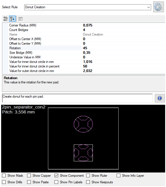
These properties are used by the StencilScriptDonut class to calculate and render the donut shape on stencil pads. The donut is typically composed of an outer arc (outer diameter) and an inner arc (inner diameter), combined with connecting lines to form a closed shape.
Ensure that InnerDiameter is less than OuterDiameter to create a valid donut. Adjust AngleStep based on performance vs. accuracy needs.
Array creation is used to replicate pad openings in a structured pattern. This is especially useful for components like QFP or QFNs,
where cooling pads are very big and replaced by array formation. The array is defined using specific rules and transformation parameters, it gives you an easy way to define an array of similar (rounded) rectangles.
| Property | Type | Description |
|---|---|---|
Array Field Count in X direction |
int | Fix Array Rule only: Array pads count in X direction. |
Array Field Count in Y direction |
int | Fix Array Rule only: Array pads count in Y direction. |
Corner Radius (MM) |
double | Corner radius for rounded elements in MM. |
Utilization Array Area (%) |
double | Utilization of avalable area in percent (only used if no fix size is used and value >0). This option will ignore the undersize value and depending to the settings it is possible the values are not exact. |
Minimum Array Field Size (MM) |
double | Array pads has minimum this size, if there is only space for one pad no array created. |
Offset to Center in X direction (MM) |
double | Fix Array Rule only: X offset to shift the array from the pad center. |
Offset to Center in Y direction (MM) |
double | Fix Array Rule only: Move array in Y direction from center of the pin. |
Distance Array Fields (MM) |
double | Array pads has this distance to next pads. |
Undersize Value in MM |
double | This value is only used if no Array size is defined. All other Elements will use this value in mm to generate undersize. |
Ignore Mask Intersecting |
bool | Do not check for mask intersecting (add all array elements without checking mask). |
Array Size Width (MM) |
double | Width for complete array, if it is =0 the original element width is used. |
Array Size Height (MM) |
double | Height for complete array, if it is =0 the original element height is used. |

These properties are used in the StencilScriptArray class to define how shapes are duplicated and transformed. Each array pattern follows a specific logic:
- check avalable size of array
- check max pad size and gap value
- split area in pads and round the rectangles
Use array rules to easily build consistent and scalable designs for components with repeated pad layouts.
Adjust offset values to fine-tune placement, it also has an utilization property to gives the rule an optimum of area.
The StencilScriptHouse class defines the necessary parameters to create a house structure around a stencil pad for solder paste applications. It is used for automating stencil generation and includes geometry, shape characteristics, and spacing considerations.
| Property | Type | Description |
|---|---|---|
Corner Radius (MM) |
double | Corner radius for rounded elements in MM. |
Offset to Center (MM) |
double | Move houses to the center of the component. |
Invert Direction |
bool | For smaller elments sometimes the house should be show away from the component. |
Undersize Value (MM) |
double | All Elements will use this value in mm to generate undersize. |
House distance cut size in Percent |
double | Value in percent depending to the height of the pad. |
Utilization House Area (%) |
double | Utilization of avalable area in percent. This option will modify the cut size value to come near to the percent value. Use 0 to ignore this value. |
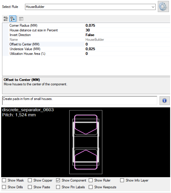
These parameters help define the geometric and contextual constraints for automatically generating stencil pad protection using a house-shaped perimeter. The house rule is recommended for chip packages, but can be used for all pins with clear directions.
Note: If the pin is under the body the direction cannot be calculated and no house is created.
Depending to the chip size it is recommended to change from house to inverted house rules.
| Property | Type | Description |
|---|---|---|
Corner Radius (MM) |
double | Rounding on the corners. |
House distance cut size in Percent |
int | Value in percent depending to the height of the pad. |
Invert Direction |
bool | For smaller elements sometimes the house fhould be show away from the component. |
Max Size of one Element (MM) |
double | Each element has maximum width and height, if the size is bigger it is automatically splitted in more elements. The value is in MM! |
Undersize Value (MM) |
double | All elements will use this value in mm to generate undersize pads. |
Offset to Center (MM) |
double | Move houses to the center of the component. |
Step for Big Elements (MM) |
double | If the element is bigger Max Element Size it use this value to split the size in more elements. |

These properties are used in the StencilScriptInvertedHouse class to define how shapes (such as stencil pads or vias) are duplicated and transformed. In general this rule is used for Chip Packages.
Note: If the pin is under the body the direction cannot be calculated and no house is created.
The StencilScriptSimpleSurface class defines the necessary parameters to create a rectangle structure around a stencil pad for solder paste applications. It is used for automating stencil generation and includes helpfull options.
| Property | Type | Description |
|---|---|---|
Corner Radius (MM) |
double | Corner radius for rounded elements in MM. |
Try Find Direction |
bool | Rotate surfaces depending to the direction of the pin. |
Rotate Bridges 45 Degrees |
bool | All bridges are rotated 45 degrees to obtain diagonal openings. |
Offset to Center X (MM) |
double | Move rectangle in X direction from the center of the pin. Or if you use negative values away from center. |
Offset to Center Y (MM) |
double | Move rectangle in Y direction from the center of the pin. Or if you use negative values away from center. |
Bridge Width (MM) |
double | Use bridges to cut the rectangle with this width. |
Bridge Count X |
int | Use bridges to cut the rectangle with count in X direction. |
Bridge Count Y |
int | Use bridges to cut the rectangle with count in Y direction. |
Offset move away disctance (MM) |
double | Move surface away from center point, this is only for outer pins (not for cooling pins). |
Size Width in MM |
double | Width for this pad. |
Size Height in MM |
double | Height for this pad. |

These parameters help define the geometric and contextual constraints for automatically generating stencil pad protection using a rectangle-based-shaped perimeter.
Note: The simple rectangle rule ignore the mask opening and overprint it!
The StencilScriptUndersize class defines the necessary parameters to create a similar structure around a stencil pad for solder paste applications with smaller size. It is used for automating stencil generation and includes geometry, shape characteristics, and spacing considerations.
| Property | Type | Description |
|---|---|---|
Undersize Value in Percent |
double | All Elements will use this percent value on the smaller side to generate undersize. |
Undersize Value in MM |
double | All Elements will use this value in mm to generate undersize. |
Corner Radius (MM) |
double | Corner radius for rounded elements in MM. The value is independent of the undersize and can change the earthings with different values. |
Max Size of one Element (MM) |
double | Each element has maximum width and height, if the size is bigger it is automatically splitted in more elements. Value is in MM. |
Steg for Big Elements (MM) |
double | If the element is bigger MaxElementSize it use this value to split the size in more elements. Value is in MM. |
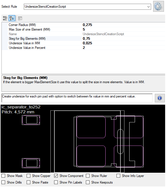
These parameters help define the geometric and contextual constraints for automatically generating stencil pad protection using a smaller-shaped perimeter.
Note: If the undersize values to small no pad will be created, the rule checks the mask layer for intersecting!
The StencilScriptUsePinMinusMask class defines the necessary parameters to create a pin bases structure. It is used for automating stencil generation and includes geometry, shape characteristics, and spacing considerations.
This rule gives you the option to use the pin outline as basis with following options:
| Property | Type | Description |
|---|---|---|
Undersize Value in Percent |
double | All Elements will use this percent value on the smaller side to generate undersize. |
Undersize Value in MM |
double | All Elements will use this value in mm to generate undersize. |
Overwrite All Pins |
bool | Overwrite all pins regardless of the underlying pads. Set this property to false if you want to change single pins with different rules! |
Corner Radius (MM) |
double | Corner radius for rounded elements in MM. The value is independent of the undersize and can change the earthings with different values. |
Ignore Mask Layer |
bool | Take Pin without Mask Intersecting! This do not check overlappings and openings in the mask layer. |
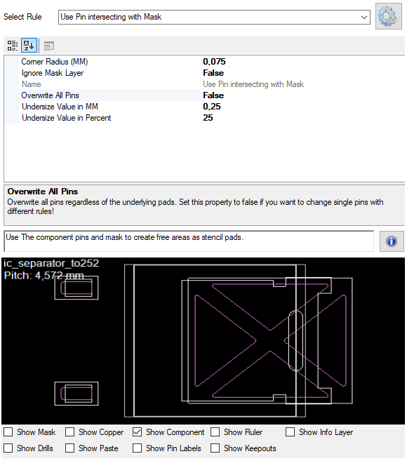
These parameters help define the geometric and contextual constraints for automatically generating stencil pad protection using the pin definition as basis.
Note: If the undersize values to small no pad will be created, the rule checks the mask layer for intersecting and it is a special handling for Overwrite All Pins to replace all pins with one rule!
Export tespoint foil as PDF or print it.

The export looks like this:
All Labels are searchable in the PDF, for panel it counts up after the first PCB.
Import component attributes and properties from csv/excel files:

There are some options to set variants, no pop and comp ignore attributes. Depending to the containing components all others are ignored and/or set no_pop. The variants set/add for all included components so it is easy to handle different placement variants by loading different excel/csv files.
Depending to your attribute file you can connect it via Reference, Part Number, Package or free propertes (e.g. MPN or VPN).