| Format | Import | Export |
|---|---|---|
| ODB++ | x | x |
| GenCAD 1.4 | x | x |
| CC/CCZ | x | - |
| Fabmaster (Cadence Allegro Fabmaster, or FABmaster) | x | - |
| Eagle | x | - |
| IPC-2581 A/B/C | x | x |
| Gerber RS-274-X | x | x |
| DPF | x | - |
| IPC-356 | x | x |
| DXF | x | x |
| IDF | x | x |
| IDX | - | x |
| Sieb & Meyer | x | x |
| Excellon 1,2 | x | X |
| Image files (JPEG, PNG, BMP, GIF, TIFF) |
x | x |
| CSV (e.g. MS Excel, Txt-Lists) |
x | x |
| AVL | x | - |
| x | x | |
| 3D formats: 3Ddata as obj/vrml files |
x | x |
| STEP | x | x |
| SVG | x | x |
| 3D PDF | - | x |
| WebGL | - | x |
| Mentor Pads | x | - |
| Many Machine Formats | - | x |
| Any ASCII Format | - | x |
| Format | Data type | Component | Nets | Stack up | Wiring layout | Additional info |
|---|---|---|---|---|---|---|
| ODB++ | folder | x | x | x | x | x |
| Eagle | folder | x | x | x | x | x |
| GenCAD | 1 file | x | x | x | x | x |
| IPC-2581 a/b/c | 1 file | x | x | x | x | x |
| CC/CCZ | 1 file | x | x | x | x | x |
| Fabmaster | 1 file | x | x | x | x | x |
| Gerber | 1 file per layer | - | - | - | x | - |
| DPF | 1 file per layer | - | - | - | x | x |
| DXF | 1 file per layer | - | - | - | - | - |
| IDF | 2 files | x | - | x | - | - |
| IPC-D-356 | 1 file | - | x | - | - | - |
| AVL/CSV | 1 file | x | - | - | - | - |
| 1 file | - | - | - | - | - | |
| Pads | 1 file | x | x | x | x | x |
CAD and CAM systems are often produced by different companies, so, it is necessary to agree on a CAD-to-CAM data exchange format. ODB++ is such a format and arguably the closest to a global industry standard. Developed and released by Valor Computerized Systems, Ltd. in 1995, it was and still is continuously improving to meet the evolving needs of PCB designers, fabricators, and assemblers.
In 1997 together with component names the ++ suffix was added in reference to C++ and in 2000 development of an XML version started, which ended in 2008 when this new ODB++ format, called ODB++(X), was donated to the Association Connecting Electronics Industries (IPC) in an attempt to merge GenCAM (IPC-2511) and ODB++ into a new format called IPC-2581. ODB++ is the de facto standard for intelligent PCB data exchange containing all data necessary to fabricate, assemble and test in a single hierarchical file structure which makes it superior to the only format more popular: Gerber.
Some of the major benefits of ODB++ include:
The aforementioned reasons explain why ODB++ is the standard format of PCB-Investigator, which is always used internally even if the data were imported in a different format.
AutoCAD DXF (Drawing Exchange Format) is a widespread file exchange format for CAD data developed by Autodesk, Inc., that enables vector data exchange as well as 2D and 3D graphics drawing. Originally introduced in December 1982 as part of AutoCAD 1.0, it was intended to provide an exact representation of the data in the AutoCAD native file format DWG (Drawing), but since Autodesk didn't publish its specifications until many years later, correct imports of DXF files have been a problem since the beginning. Another problem is that DXF typically is dimensionless meaning it doesn't provide all necessary information to permit interoperability with other programs. That's why it's essential that the viewer knows the unit that was used to produce the drawings. With AutoCAD supporting more complex data types over the years, DXF has become less useful but due to its good documentation and with being the lowest common denominator of all CAD based systems, it is still quite popular and therefore also supported by PCB-Investigator.
The DXF Export has following options:

1) You can combine all active layers in one file or only one layer
2) It is possible to write multi files while the export
3) Switch the unit and the outline mode
4) It is possible to split all arcs in lines by fix length value. This can be filtered only for areafills/surfaces.
5)List of additional options:
- Export only selected objects instead of complete layers
- Combine objects to nets, this remove overlappings and export only the combine outline.
- Use DXF Layer per Package, to export one layer foreach package type.
- Add profile contour, adds the contour to the file(s).
- Add Pin Labels to switch the pin label to ignore.
- Write CMP-References, add text foreach component reference.
- Add Notes, export note objects.
Among ODB++ and IPC-2581 GenCAD is one of the most important file formats for PCBs. The primary focus of the GenCAD standard rests on fabrication and testing. GenCAD contains all information about a PCB ranging from net, component and route information, to complete layer setups in a single file which provides additional protection from data loss.
In some software you have export options, for a good result (e.g. for bottom side components) use e.g. this setting in target software: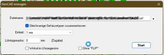
(angle counter clockwise and no flip option)
The Intermediate Data Format (IDF) is a 3D CAD data exchange format which is specifically designed for the import and export of PCB data. It consists of two files, a component library (* .emn) and a layer assembly file (* .emp). The component library file contains information about the PCB dimensions (PCB outline), the position and orientation of the components, the position of the mounting holes, cutouts and the barrier areas, the layer assembly file contains information about the file dimensions and the height of the individual components.
The Import Dialog gives you options to use different Board and Library Files:

If you use drag & drop, both files must be in the same directory, otherwise you must use the import dialogue and specify both files with complete directory paths.
Gerber is an open ASCII vector format for 2D binary images, which allows a smooth data exchange between CAD (development) and CAM (production), since it can be imported as well as exported by all current CAD and all common CAM programs. It is particularly used to output the layout data for printed circuit boards. However, it must be noted that the Gerber format can only contain one layer per file, so multilayer PCBs must be recorded in several Gerber files. The RS-274-X extension is a two-dimensional bi-level vector-oriented image description format that includes coordinates and commands and contains a complete, unambiguous description of a circuit board. Since the format does not describe which position is displayed, it is recommended making the filename visible in the layer function . Although the export of the format provides a list of all component connections to networks and bores, no components and network data are supported. This deficiency can, however, be offset by using the IPC-D-356 network list.
If you search for instructions how to modify gerber data to run analysis and exports see this page.
The Gerber Export Dialog has many options:

1) Layers to Export can switch between "All Layers", "All Active Layers" and one selected Layer
2) You can set the number format, if you have to less trailing digits it will warn you e.g. for inexact arc.
3) Unit (Metric for mm output or Imperial for Inch output)
4) Other Options to add X2/X3 properties like layer type or net information.
5) File Name can start with the layer index to recreate the layer stackup, add the layer type to set the matrix information and use Pre Fix and your own extension.
6/7) are options how to handle removed objects e.g. flatten or repeat them. In Gerber X2 it is also possible to use Block Aperutes.
8) Additional Options:
- Export only Selected Objects to filter only some objects
- Add PCB Outline to create the profile in output file(s).
- Mirror Output e.g. for bottom side.
- Use Feature Ignore Attribute, to ignore elements e.g. all objects outside the profile has the ignore attribute.
- Export All Layers in one File, mean combine output in one file.
The Sieb & Meyer format - as well as the Excellon format; they only in a few details - was created to operate CNC drilling and milling machines. Therefore, it supports only simple attributes and drill tool definitions and is primarily used to output drill information, like for example the diameter of the holes. As a rule, each drill file also requires a separate tool file, which indicates the diameter of the tool used.
If you want to export Sieb and Meyer Files use this dialog:

You have an list for all rout and drill layers with some information like element count and Type.
Many of the options for specific other drill and routing formats and not allowed for sieb and Meyer.
You can select the standard tools for not defined elements e.g. like surfaces with routings inside.
In the Manage Tools dialog you have a list of all used tools and can manage sprcific information like Spindle speed, Retract Rate and Feedrate. You can add your own information to each tool. Depending on the format it uses the standard information on different locations e.g. by tool change or only in header.
In many cases PCB-Investigator offers the possibility of exporting data in different file formats - e.g. as lists for MS Excel, TXT, as well as detailed descriptions in MS Word or HTML - as reports. Though no real output format, reports contain valuable information for identifying potentially problematic areas. Please refer to the plugin description section in this manual for further information.
IPC-2581 ("Offspring") is the result of the aforementioned attempt to merge GenCAM with ODB++(X). Like its predecessor ODB++(X) too is XML based. Contrary to ODB++ however IPC-2581 is a common free format which is developed by 40 enterprises under the leadership of Cadence Design Systems and which specifications can be downloaded freely. In 2011 an industry consortium was created to support the development of IPC-2581, a step at least partly motivated by the fear the more popular ODB++ format could be vendor locked by Mentor at some point. These 40 companies include big names like Fujitsu, Nvidia, Cisco,... which see the big potential of the standard to prevent data transmission errors and of course save costs. Even Ucamco, the owners of the Gerber format, and finally also Mentor, the current owners of ODB++, joined the consortium.
IPC-2581 contains data about the layer structure, copper structures per layer, assembly order, material information, drill data and test points with the names of their corresponding network names and components including coordinates and rotation values for the placement. Furthermore, IPC-2581 promises to be able to document all necessary steps in one consistent record.
After last update we can import revision A, B and C.
The IPC-C export already supports generic exports for stencil, test, BOM, assembly and fabrication files. The assembly version contains simple 3D components.
IPC-D-356 is an electrical test format, traditionally used to supplement Gerber files with netlist descriptions. It was originally designed to define a standard netlist format by which bare board test information can be represented. That means storing netlist information along with XY coordinates as well as referencing pins and other components. Done right IPC-D-356 contains all information a test system would need to perform a bare board check in a single consistent file.
The AVL (Approved Vendor List) is a supplement file, which contains a list of all approved and debarred manufacturers of all PCB components. There can be multiple approved manufacturers for one component. The various approved manufacturers are usually determined by strict criteria (e.g. quality, delivery capability, delivery times, cost intensity,...) defined by the purchasing department.
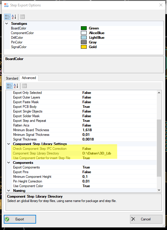
STEP (short for "Standard for the Exchange of Product model data") is a popular exchange format connecting the world of electronics and mechanics. Usually it is used to share 3D models between users with different CAD systems. STEP goes beyond the simple exchange of gemoetry like DXF and IGES. You can integrate all forms of CAD data models (wire, surface and volume models) in the geometry description.
Step Export has two detail areas, first is Standard Export:
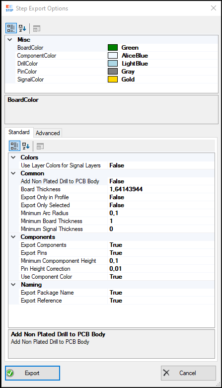
Determines whether the PCB body is exported.
Enables the export of PCB components.
Determines if component pins should be exported.
Defines the color of the PCB board. (Hidden in UI)
Defines the color of components on the PCB. (Hidden in UI)
Defines the color used for signal layers. (Hidden in UI)
Adjusts the height of pins to make them more visible.
Specifies the standard thickness of the board if no stack-up is defined.
Sets a minimum height for components when their height is zero.
Combines objects with the same net in a STEP item.
Exports only the objects within the defined profile.
Defines the global library directory for STEP files, ensuring component package names match the STEP file names.
Ensures components follow IPC rotation to match the STEP library if different from package shapes.
Positions all components at the center of CAD bounds by default.
And Second Export Options for Advanced settings:

Export the PCB body.
Export components included in the PCB design.
Export component pins.
Color of the PCB board.
Color used for components.
Color used for signals.
Color used for drill holes.
Color used for pins.
Adjustment for pin height to make them more visible.
Standard board thickness if no stack-up is defined.
Standard layer thickness if no stack-up is defined.
Minimum component height if component height is set to 0.
Minimum board thickness.
Minimum layer thickness for signals.
Minimum arc radius to be exported.
Option to export outer layers of the PCB.
Option to export inner layers of the PCB.
Export only the selected objects.
Use ODB-specified colors for signal layers.
Use the specified component color.
Export reference to the STEP part.
Export package name to the STEP part.
Export net name to the STEP part.
Combine objects with the same net into one STEP item.
Flatten arcs to lines during export.
Export prepregs as layer objects.
Export signal layers in a separate file.
Export component layers in a separate file.
Export signal layers without thickness.
Export drill layers without thickness.
Export drill layer.
Export all visible layers.
Export solder mask layer.
Export paste mask layer.
Export only objects within the profile.
Add non-plated drill holes to the PCB body.
Add routing layers to the PCB body, creating cutouts from panel builder.
Check for sub-steps and export all elements for a complete panel.
The layer that contains the recess elements for the top side of the PCB body.
The layer that contains the recess elements for the bottom side of the PCB body.
Path to the global library for STEP files, using the same name for the package and STEP file.
Activate IPC rotation correction for components if required by the step library.
Insert components at the center of CAD bounds by default.
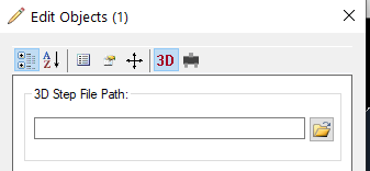
the new step import converts 3D step files in 2D slices. You can handle complete layers (e.g. with routings or drills), single step files for components (or package definitions), extra electronic and all other step files e.g. housings.
You can use the imported step files for 3D generation (connected to the original step file), it is possible to place the import many times or as replacement for the step export.

In the Step Import dialog you have some options e.g. rotate/scale/translate and auto adjustment (Set Center (0,0)). You see the slice plane in light blue and can also add the CAD data Board outline for exact placing.

(screenshot 3D PCB in adapter with extra electronic and fixing pins)
Eagle (short for Easily Applicable Graphical Layout Editor) is the native format of Autodesks schematic editor (also named Eagle) for designing PCBs.
The PCB-Investigator Eagle import reads the brd-File with all nets and components as well as board layers. The layer information is approximated and not intended for PCB production.
The algorithm for flooding area fills and connecting thermal ties may differ from the original Eagle algorithms!
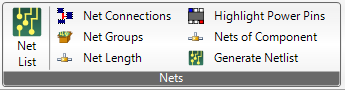
The NetGroup Wizard can be used to create net groups and to add or remove nets to them.
Open the NetGroup Wizard with clicking the "Net Groups" button.
The following dialog will show up.
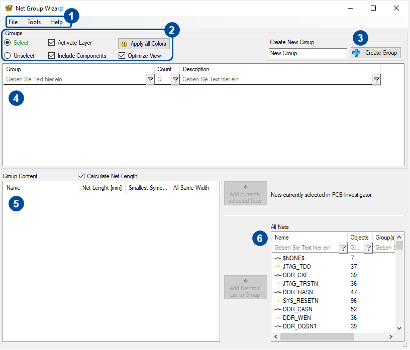
1. The two important tabs contain the following options.
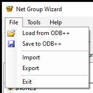
The net groups are always stored within the ODB design. Sometimes, you want to import net groups from another design. Prior to that, export the current net group to have a backup of them. In the import you can select between different file formats (xml, txt, dcf, dcfx, csv, rulf) to add net groups from other software (e.g. Xpedition or Zuken) or if you select xml from other PCB-Investigator exports.
Import Format List:
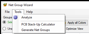
The "Tools" tab has three important functions.
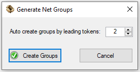
To create net groups, the net names will be used. The number is the number of letters to be tapped. All nets with the same beginning will then be added to the net group. The net groups names depend on the tapped letters.
2. The summary of controls allow you the following operations:
3. The button "Create Group" allows you to create you own groups with the desired group name.
4. This control contains all net groups which are deposited in the ODB dataset. More options to edit net groups can be found by right clicking on a net group.
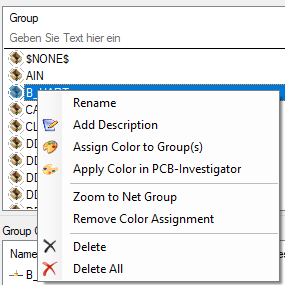
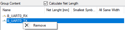
5. Every net of the net group will be shown here, if a group in the group view (4) is selected. To remove a net of the net group, right click the net you want to remove and click remove.
6. If y net group (4) is selected, you can add single nets to the net group with clicking a net in the view with the number 6 and clicking the add button. There are two different add buttons:
For more details have a look to this short video:
To import components, you can use the Component (CSV) Import.
This works for all excel or CSV files with References and X/Y positions. If you have only BOM Information you have to use the Part Matcher

The import is easy to use, PCB-Investigator will try to find the columns but user can modify the table indizes manually.
The settings gives you options to identify the packages and place new components with different methodes:

1) options depending to the import table e.g. the unit of X/Y coordinates or the rotation direction (clockwise or counterclockwise).
2) Use existing libraries e.g. the easylogix shared EPackLib to find package outlines and optional part information (with option to set missing packages by part outlines).
3) Package Finder gives many options how to identify the packages, with "Check for Similar Package Names" small nameing differences e.g. 0603C and 0603_C handled identically. Most Important for exising footprint layer is the compare of package footprint with existing pads.

In the Results tab you have some more options:
1) Check each placed package in the Result list, there are markings for Missing/Created and Updated packages
2) Compare with the library, the founded result list (Alternative packages with score) and directly compare all placings in the design
3) Edit the result or replace missing dummy packages with different libraries. You can also create new packages via pad selection with "Create Package from Selection"
Here a short video with the complete workflow:
To view the BOM, use the Component Manager (see Working With Components or here).
To export and print the BOM, use the "Export" tab.

If you want to transfer the components to an other design, you can use the Component List Export and on the other side the CSV Import (see above). But this is only working if you store your package/part definition in an library.
CC/CCZ is the native format of CAMCAD Professional

The czz import options contains some special cases depending to known format special cases. e.g. import the custom colors.
Some of the options contain extra information and handle e.g. unknown object sizes. In all cases this import is changed for ODB++ file data and cannot handle all information in the same way like CAMCAD it do.
A '.fab' file is the native format of 'Cadence Allegro Fabmaster', or of 'FABmaster'. Both tools export '.fab' files, but with different content and definitions. PCB-Investigator can import both.
Cadance Fabmaster (.CAD) contains component, package and layout information (incudling nets). It can contain silkscreen layer with text and documentation layers with additional information. It also has drill information and some simple properties.
Fabmaster (.fab) contains components, padstacks, testpoints and net information. Thereare different shapes similar to ODB++ available and handles all important layers in simple way. For the import there are different surface options, you can switch between Close the tracks, combine touching elements and try to close them or let everything as it is.

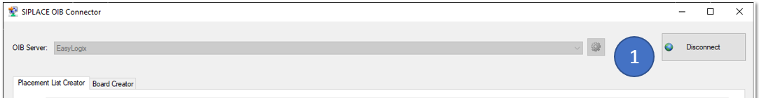
When you open the "SIPLACE OIB Connector" (in the 'Machine Export' menu) the first time, you have to first enter your OIB server settings by clicking on the gear button (1):
Following dialog will open:
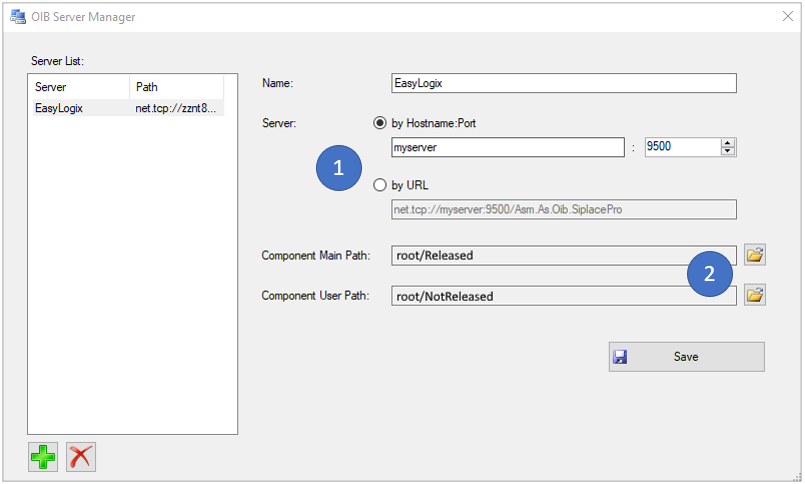
In this server manager, you can organize multiple OIB servers. To create a new one, please press on the little green "+" button and enter a name.
Afterwards you'll have to specify the OIB server adress by entering an IP/Hostname + Port, or directly enter the 'net.tcp://...' adress (1).
When this is done, you'll have to specify two server directories by clicking on the small browse button (2):
Click "Save" and close the dialog to preceeed.
To start, please select a server and click "Connect" (1).
With the "Placement List Creator" tab, you can create placement list elements for each component side on the OIB server.
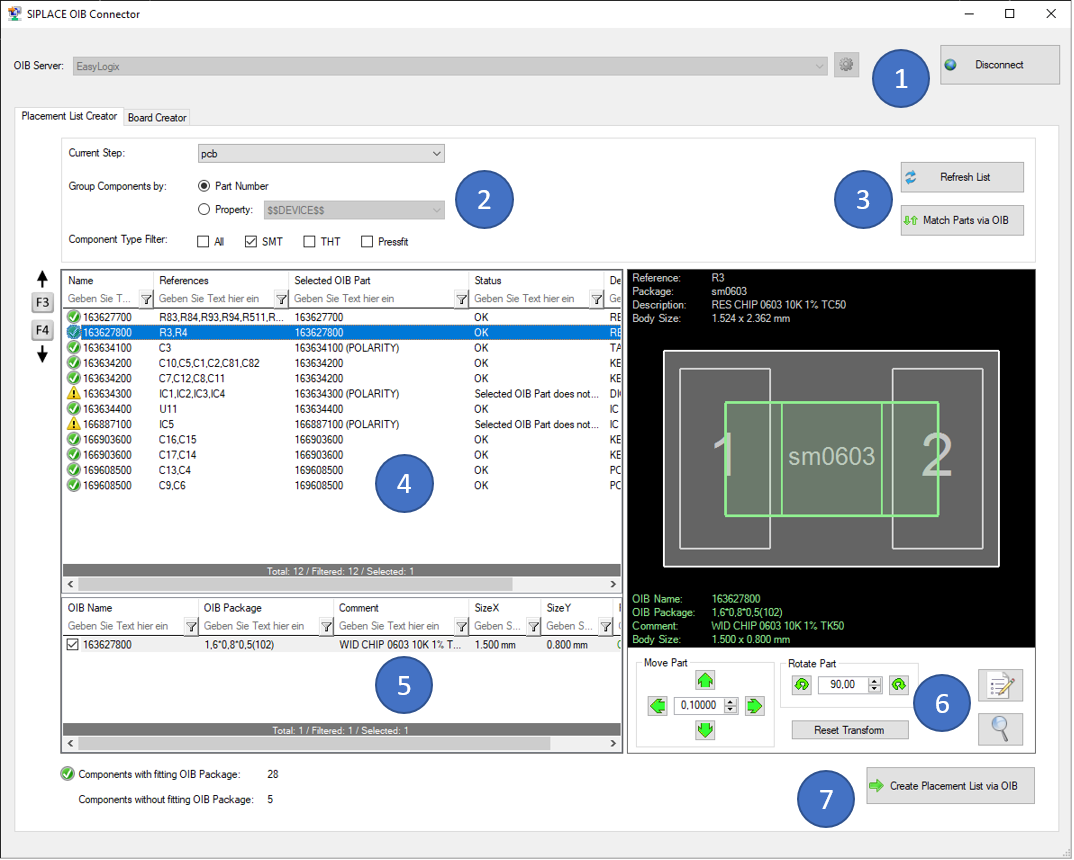
To start, you have to do a few settings in block (2):
Always when you change settings in (2), you will have to 'Refresh' the list and 'Match Parts via OIB' again (3).
When the matching process is done, you will see all your filtered parts in the list (4), including an overlay of the matching OIB part definition on the selected server. Found OIB parts are centered on the CAD package center. Details of the found OIB part and the fitting state are listed on the bottom side (5).
The 'Status' column indicates, whether a OIB part was found or not, and if the found part fits onto the CAD package. The condition for fitting is, that the pin definition of the OIB part must at least partly overlap the CAD package pin.
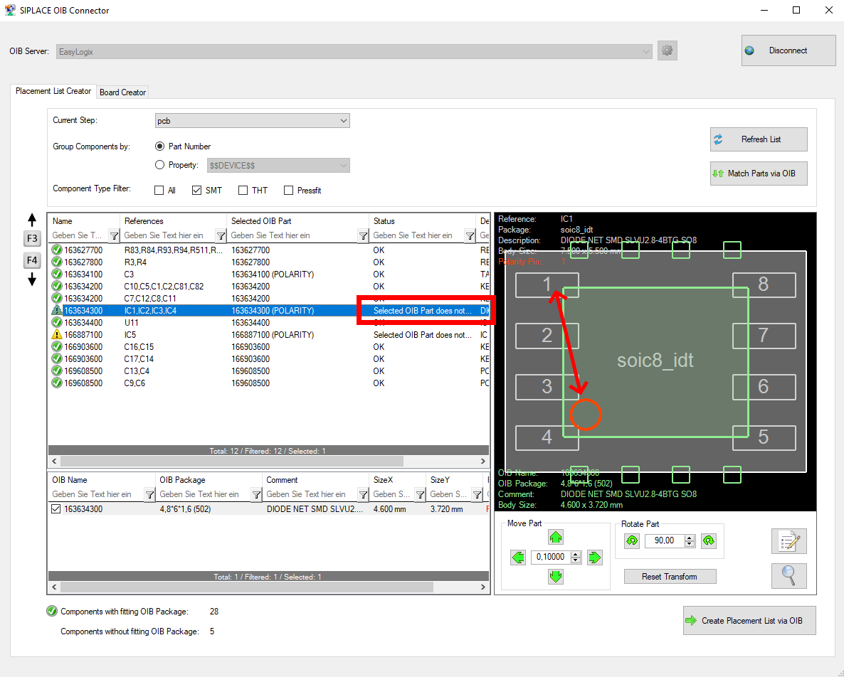
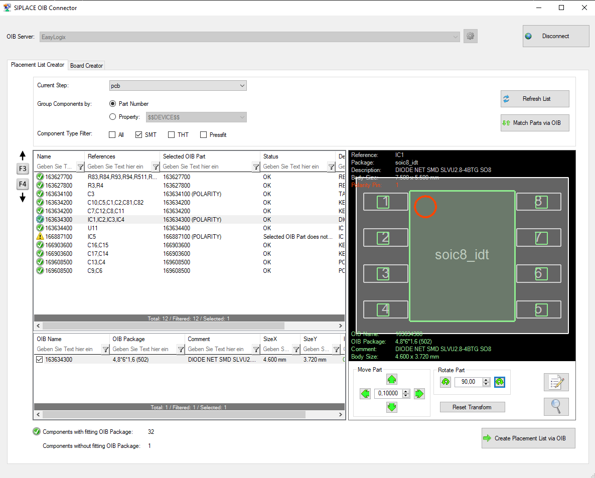
If the found part does not fit, you have the possibility to shift its position or to rotate it until it fits (6). With the two buttons in this block on the right, you can open the property dialog of the CAD component or zoom to it.
If the OIB part has a polarity definition, this polarity marker is visualized in red. The fitting alorithm then also uses the polarity information, to recognize if the component is correctly rotated (CAD polarity pin is same as OIB polarity pin).
Example of the fitting process (6) (by rotating 90° clockwise):
 =>
=> 
When clicking the 'Create Placement List via OIB' button (7), you are asked to select a folder on the OIB server and enter the name for the placement list(s) for top and/or bottom side. Afterwards, the placement lists are created via OIB. Missing parts, that where not found during the matching process, are automatically created in the 'Component User Path' (see 'OIB Server Manager'). Those created parts are dummy parts without any real outlines or pin definitions. Their information must be completed by the user in the SIPLACE Software afterwards. Components that have the ".comp_ignore" attribute are marked as 'omitted' in the placement list.
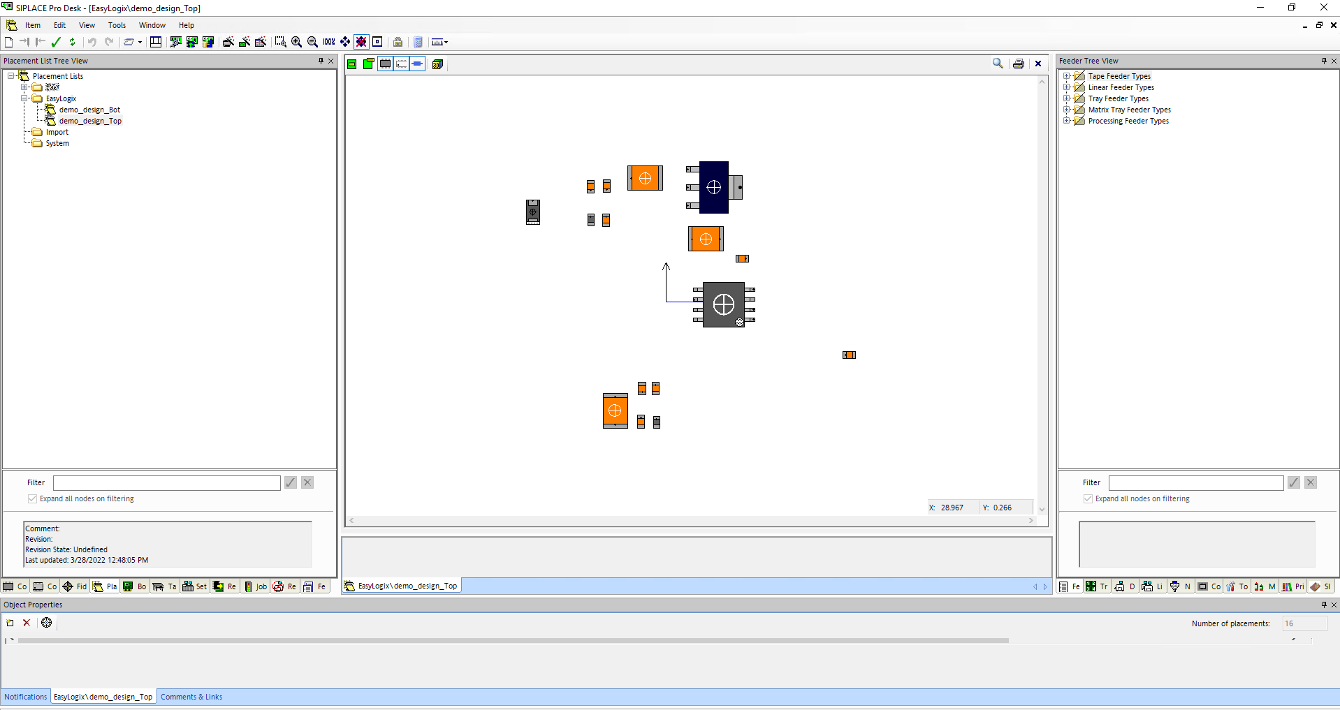
Here is a screenshot of the result in the SIPLACE Software:
After having created the placement list of the single board(s), you can create the panel data with the "Board Creator" tab.
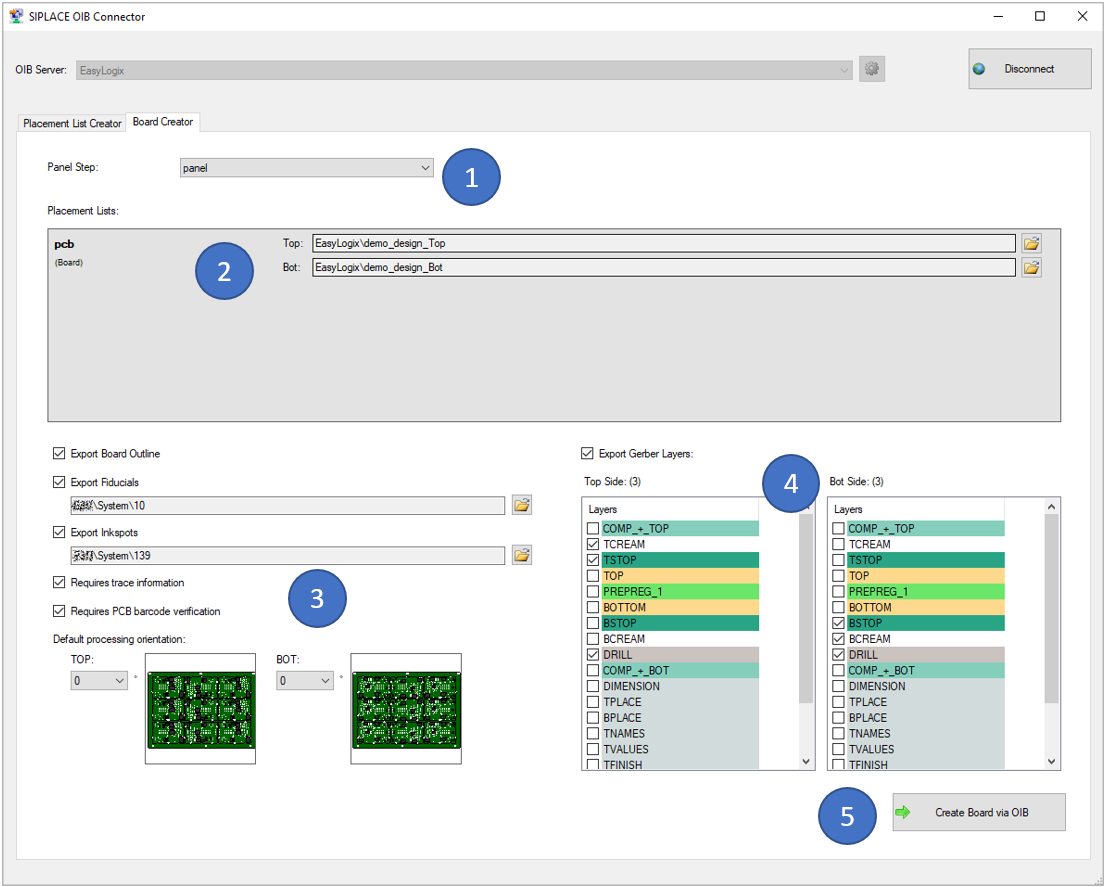
To start, you have to select the panel step that should be created (1). It is also possible to create panels in panels (recursive), when the most outer panel is selected.
For the given panel, the included single board(s) is/are listed unter (2). Here an already existing placement list on the OIB server must be selected per board and side. If the placement lists where created before in this session with the "Placement List Creator", the information is already prefilled. If not, you can click the small browse button and select the right placement list.
In the block (3), there are different options available:
In the block (4), you can choose which CAD layers should be exported and imported in OIB for this board per side. It is mainly thought for paste/mask layers.
When clicking the 'Create Board via OIB' button (5), you are asked to select a folder on the OIB server and enter the name for the board entry. Afterwards, the board is created via OIB.
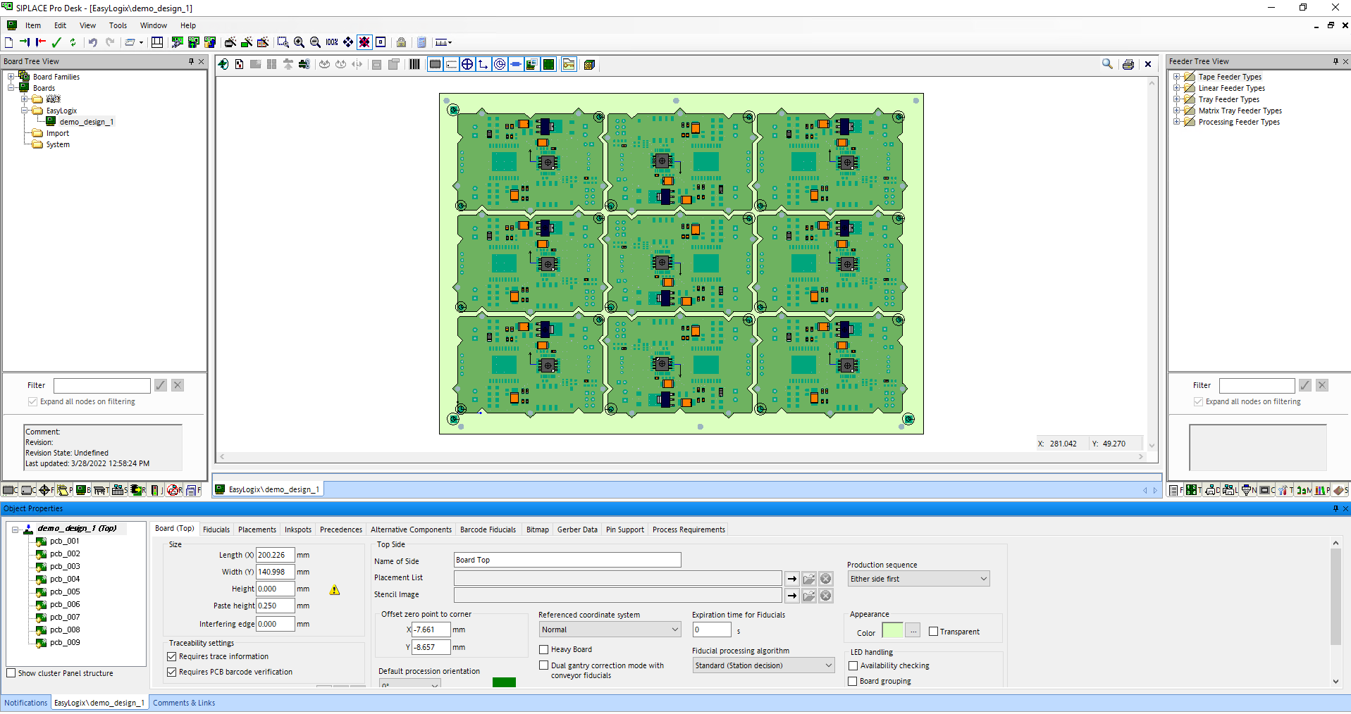
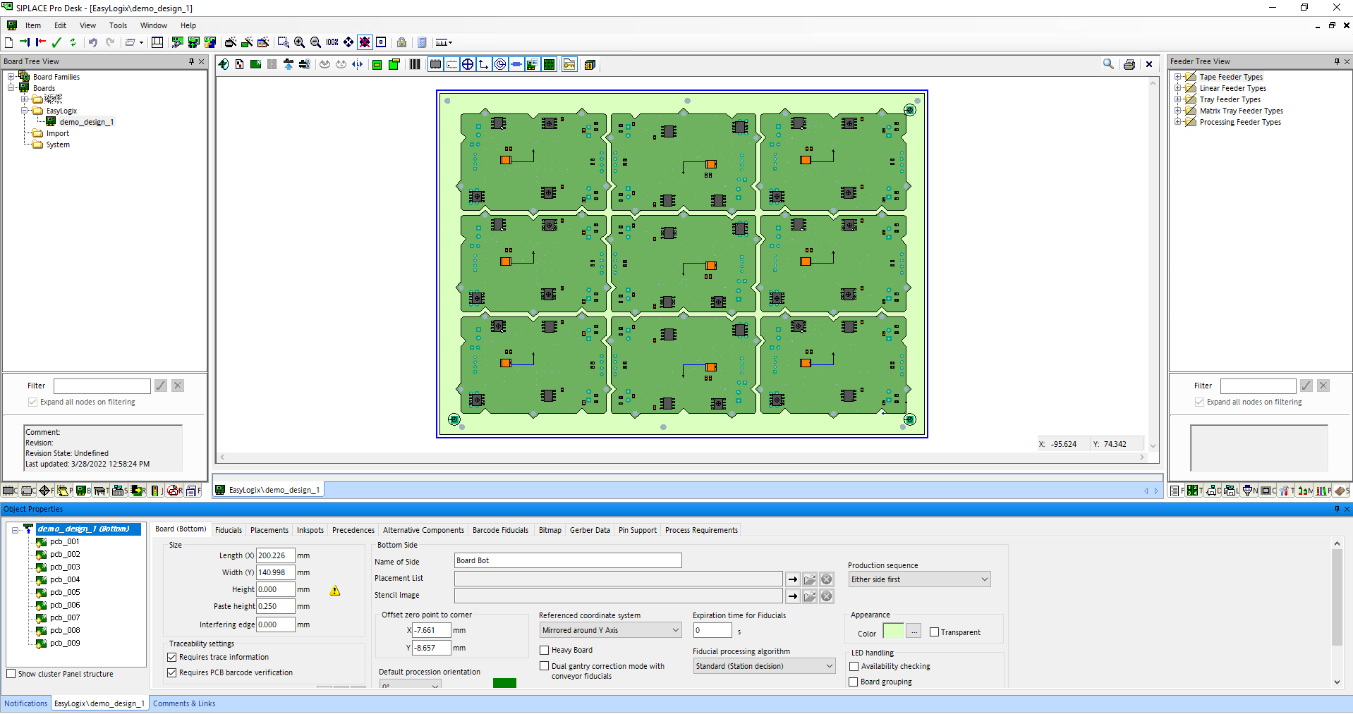
Here is a screenshot of the result in the SIPLACE Software:
With the "SIPLACE QD Exporter" tool, you can create '.qd' files including placement lists and board information for ASM machines.
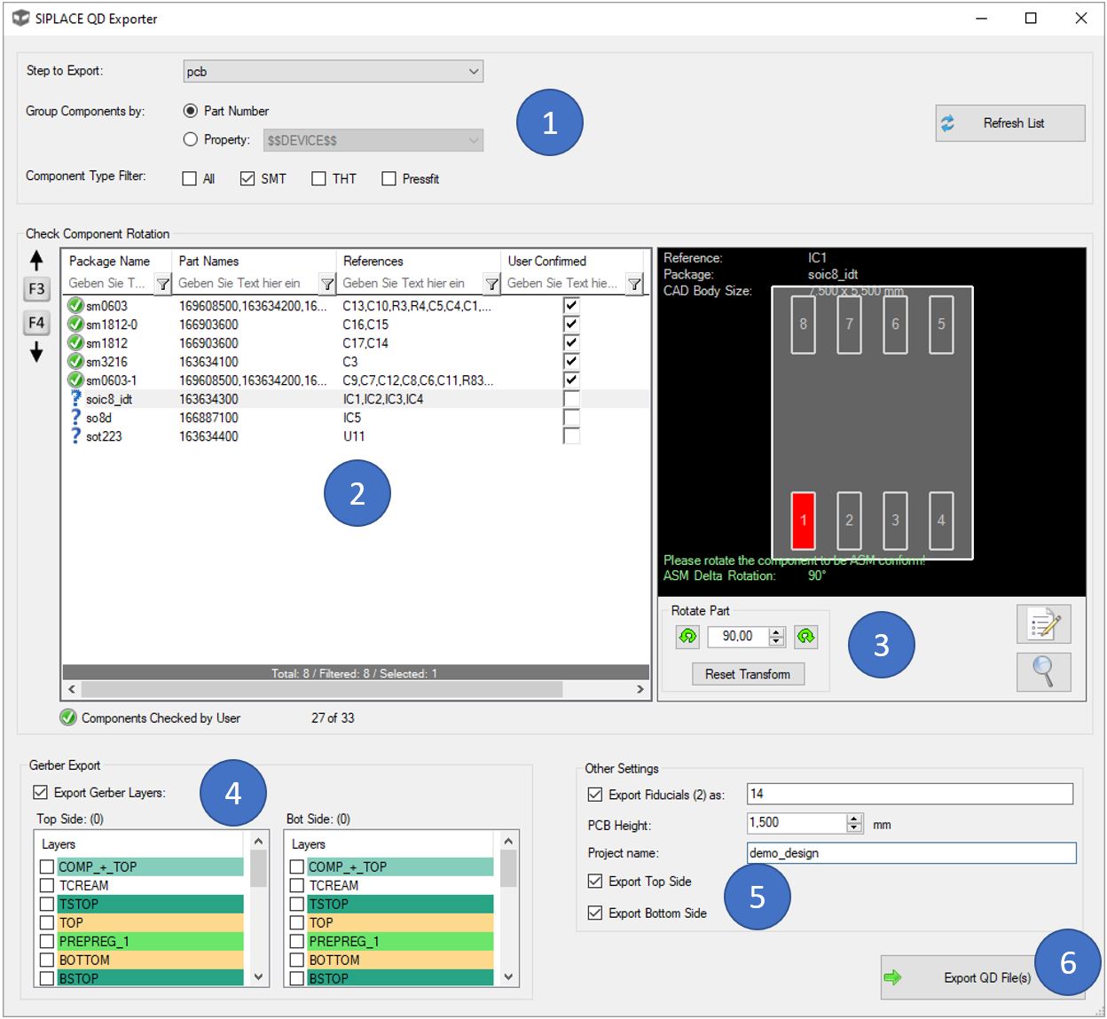
To start, you have to do a few settings in block (1):
Always when you change settings in (1), you will have to click at 'Refresh' to update the list. In the list (2), you will see all packages and the corresponding parts for each step or sub-step of your selected (panel) step.
It is then important so select list entry by list entry to check the rotation correction. If a entry is selected, you'll see the package drawing on the right side. You have to rotate this package to be displayed in exactly the same way, as it is defined on the ASM machine ('make it ASM conform'). You can confirm this by checking the "User Confirmed" checkbox in the list's last column. The rotation can be done by using the buttons in (3). Here, the rotation can also be reset and with the two buttons in this block on the right, you can open the property dialog of the CAD component or zoom to it.
In the block (4), you can choose which CAD layers should be exported as gerber files next to the '.qd' file. These gerbers can then be also imported in SIPLACE. The mirroring/translation of the bottom gerber is already done in the gerber itself, so that you do not need to transform the layers in SIPLACE.
In the block (5), there are different options available:
When clicking the 'Export QD File(s)' button (6), you are asked to select a folder where the files are exported to.
Here are some screenshots of the result in the SIPLACE Software:
| ID: 1 | Import GenCad file |
Params: string importPath |
| ID: 2 | Export GenCad file |
Params: string exportPath |
| ID: 1 | Import IPC2581b file | Params: string importPath |
| ID: 2 | Add or modify Stackup | Params: string/IFileData exportPath |
| ID: 3 | Export Stackup | Params: string/IFileData exportPath |
| ID: 4 | Export to IPC2581b file | Params: string/IFileData exportPath |
| ID: 1 | Import DXF file |
Params: string importPath |
| ID: 2 | Change Settings as XML |
Params: stringimportPath |
| ID: 3 | Save DXF file |
Params: IFileData filedata Dictionary<double, List PCBI.MathUtils.PointD> outputElements IStep step string outptLayerName bool? unitInch bool unitInch
|
| ID: 4 | Export file Asynchronus |
Params: string name XMLSettingsOutput outputSetting List ILayer outputLayers IStep step bool param
|
| ID: 5 | Export in DXF format |
Params: string exportPath IStep step List ILayer outputLayers XMLSettingsOutput outputSetting bool param |
| ID: 1 | Export SiebUndMeyer |
Params: string exportPath PointD zeroOffset double settingDouble bool settingBool Dictionary<double, List PCBI.MathUtils.PointD> excellonSpecialOutput MoveRoutingDirection routingOptionDirection XMLSettings _settings string layerNames
|
| ID: 2 | Export Excellon2 |
Params: string exportPath PointD zeroOffset double settingDouble bool settingBool Dictionary<double, List PCBI.MathUtils.PointD> MoveRoutingDirection routingOptionDirection XMLSettings _settings string layerNames
|
| ID: 3 | Export Posalux |
Params: |
| Params: string exportPath | ||
| ID: 2 | Export Viscom XML | |
| ID: 10 | Export Parmi | Params: string exportPath |
| ID: 11 | Export Goepel | Params: string exportPath |
| ID: 12 | Export Modus | Params: string exportPath |
| ID: 13 | Export Yamaha | Params: string exportPath |
| ID: 14 | Export Tri | Params: string exportPath |
| ID: 15 | Export Mycronic Data | Params: string exportPath, bool exportTHTs |
Example: parent.SendMessage("PCBI_MachineFormats_ImportExport.PCBI_Connection", "script", 1, listParams);
| ID: 1 | Export Step file |
Params: string outputStepName |
| ID: 10 | open dialog and show it | Params: string param |
| ID: 2 | show DRC dialog | Params: string param |
| ID: 3 | run check and save result file | Params: string fileName |
| ID: 1 | Export HTML with all options | Params: string exportPath |
| ID: 1 | Export result in user DIR with given Nets | Params: string outputPath |
| ID: 1 | Open the Dialog | Params: string fileName |
| ID: 2 | Save FilePath | Params:
string fileName |
| ID: 1 | Export CSV in User Dir | Params: string fileName |
| ID: 1 | Import IDF file |
Params: string importPath |
| ID: 2 | Export IDF file |
Params: string exportPath |
Example: parent.SendMessage("PCBI_IDFFilter.PCBI_ConnectionImport", "example", 2, new List object(){"path"}
| ID: 1 | Add Rule File |
Params: string importPath |
| ID: 2 | Run rule check |
Params: string resultPath |
| ID: 3 | Open net group dialog |
Params: string info string |
| ID: 4 | Open net rule dialog |
Params: string step name |
Example: parent.SendMessage("PCBI_NetGroups.PCBI_Connection", "example", 4, new List object(){"stepname"}
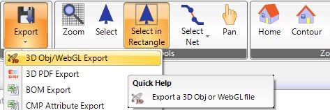
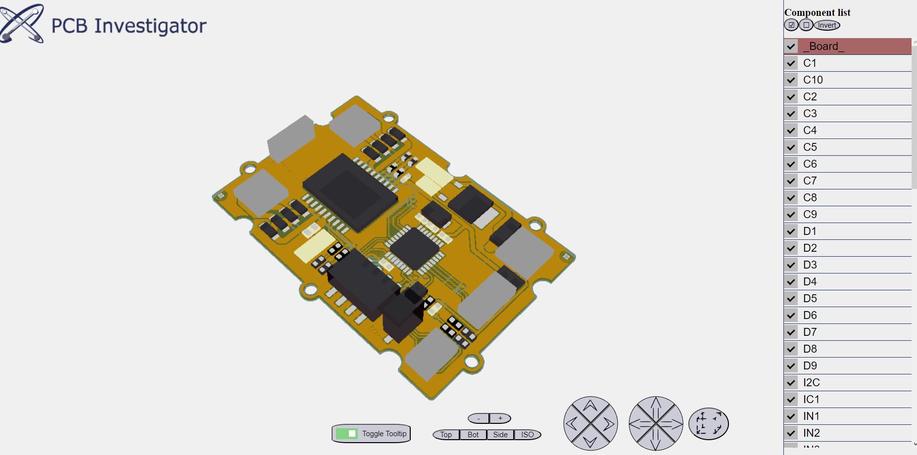
If you wish to export your 3D design, you have the option to do so in STEP, OBJ, STL and WebGL formats.
see more to step format here!
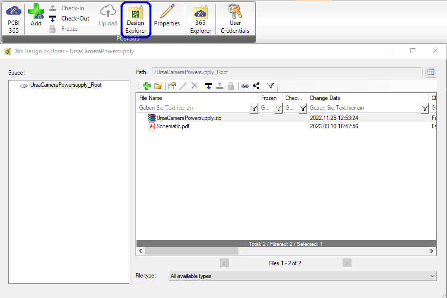
365 Explorer to check all files in the storage, including designs and all additional files
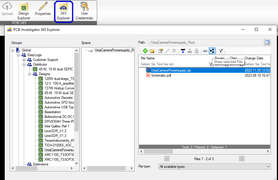
Open PCBI 365 design tree
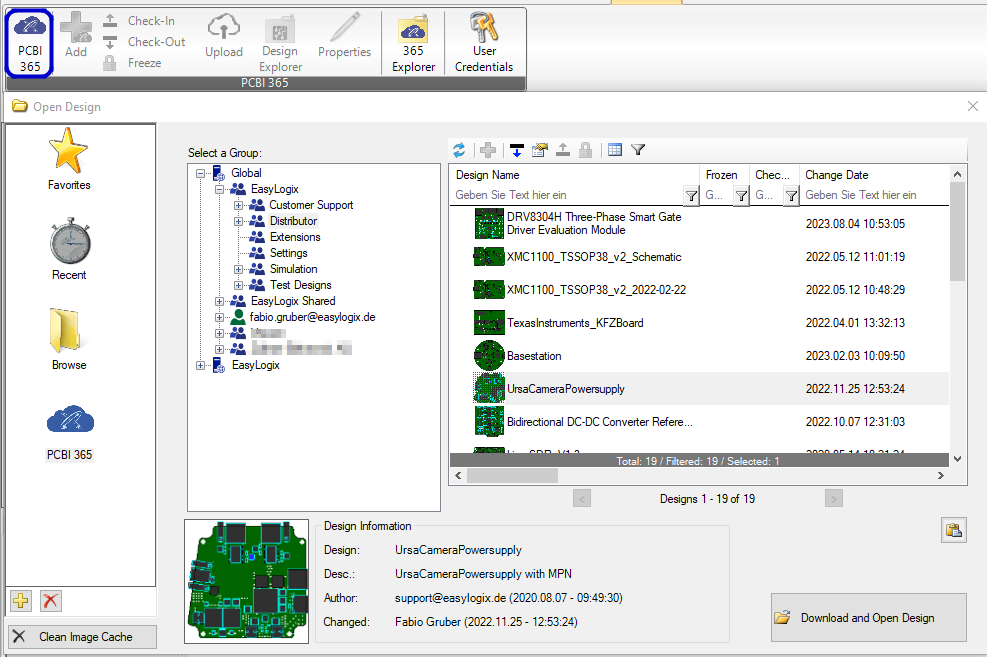
1) The Group tree with all available groups
2) Add current design to the selected group
3) See design properties
4) Define visible columns (here Design Name, Creation Date,...)
5) Filter visible designs
6) See history for selected design, more detailse here
Add current design to the 365 cloud
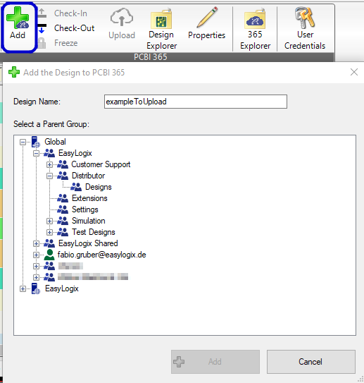
Select path to 365 group and add the open design.
With the Design Explorer you have an overview all additional files for this data stored. E.g. additional BOM files, Images, schematics, exportes and notes
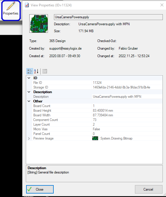
Design Properties to find the design later again (including comments, design size, layer count)
Upload data to update the design online
Panel Builder brings an template manager with it, there are options to store panel templates and an coupon library online or local.
With the templates you can use standard panel sizes with fix drill and marker positions. It is possible to store templates for each layer count, depending to the size of the useable area it calculate the amount of single PCBs in the template.
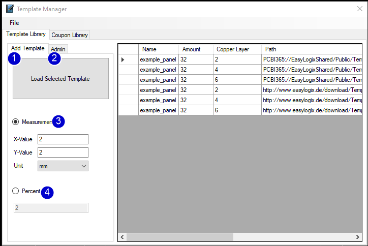
1) Add Template from the list on the right side
2) Change to Admin area
3) Options for distance in fix values
4) Option to fit single pcb with percent distances
Admin Area

1) Add the current design as template to the list.
2) Remove the selected template from the list.
3) Open the update dialog with many more options (useable ares, copper layer count, path to the template and step name)
Coupon Library
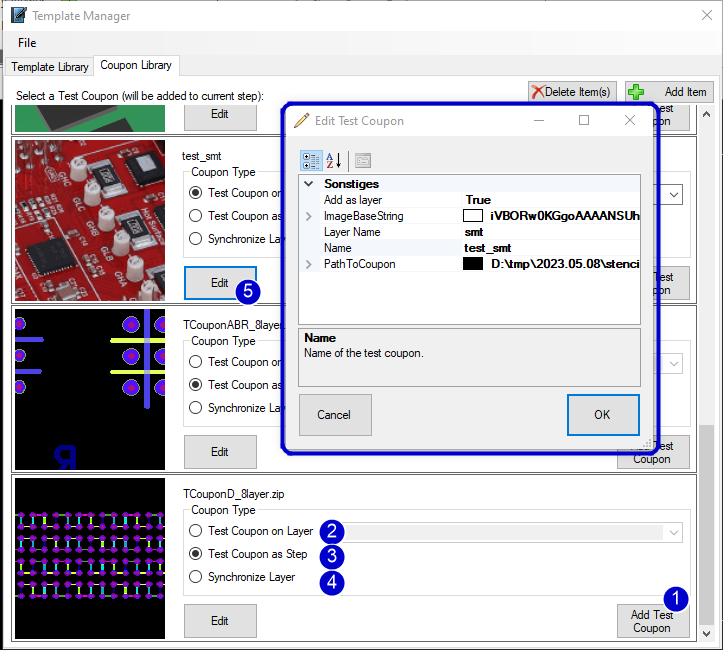
1) Add the selected coupon to the panel.
2) select "Test Coupon on Layer" to add the loaded coupon entry on one layer.
3) select "Test Coupon ad Step" to create an new step with all coupon information (recommended for coupons with components and net information)
4) select "Synchronize Layer" to fit the coupon data on the panel layers.
5) Edit the coupon entry, e.g. change image or path to the coupon.
Here is an example how the report can be organized, with extra tab pages for each exported analysis:

The report begin with an overview for each step with e.g. design size, component count and the stackup information (signal layers, step count, layer count, net count,...)
With the extended design report you can use customization to change colors and images, you can also add own reports and pages. The report has an open Interface to automate it and create complete reports for all made analysis/checks.
Here is an example extended design report:
Export Parmi Files for SPI/AOI with component, package and pad information (including polygon outlines and standard shapes like rectangles and circles).
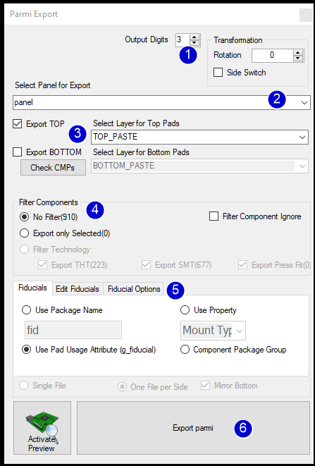
1) options for output digits and transformation (e.g. export your board with 90 degree rotation)
2) Select the output panel
3) export Top and/or Bottom side with extra layer for the paste definitions
4) use filters e.g. for THT components or ignore unplaces components
5) change the fiducial definitions and options
6) Export the Parmi PADX File(s)
Export Viscom vVision and older Formats for AXI, AOI and SPI machines

1) Export Type and generall settings
2) Export Panel and options for sides (for AXI combined file for both sides possible), you can also select the paste layers for top and bottom side here
3) Set component Attributes, many output elements need further information e.g. you have to define the package group to export BGAs, SOICs and CHIPs in simple form
4) Define the output project name
5) Filter components e.g.g export only SMT components
6) Define Fiducials and Bad Marks or change there definitions
7) Optional use of global output libraries
8) Depending on the machine type you can add camera marker
9) Depending on the machine type you can add laser marker
10) Export SPI or vVision format
The Viscom export has many option e.g. for specific viscom machine types with laser marker or camera marker, it supports mapping files aswell as library structur for cle and cad files.
Here is the list of all export options you can modify for viscom files:

1) generell options like output digits in the files or use naming confentions for package group footprints in cle files.
2) tolerance and file/folder naming
3) copy default files for specific cases e.g. copy par or si_lpos files and alias files handled different for AOI/AXI and SPI
4) use mapping and update the file
5) fiducials replaced by rectangles or TAR files for AOI/AXI and SPI
6) many options for output files like output folder in SI structur, SPL Files for splitter definition or the rotation system.
7) specific options for vVision (xml) files like automatically library update with lead information, use mpn packages from library or replace step names by numbers and some more
The expert options contain many options that you define once and cannot change later. You must have a certain amount of background knowledge to be able to use some of these options!
Export Siplace QD Data or connect ot OIB machine
more details for OIB here:
https://manual.pcb-investigator.com/pages/siplace_oib_connector
and more details for QD here:
https://manual.pcb-investigator.com/pages/siplace_qd_exporter
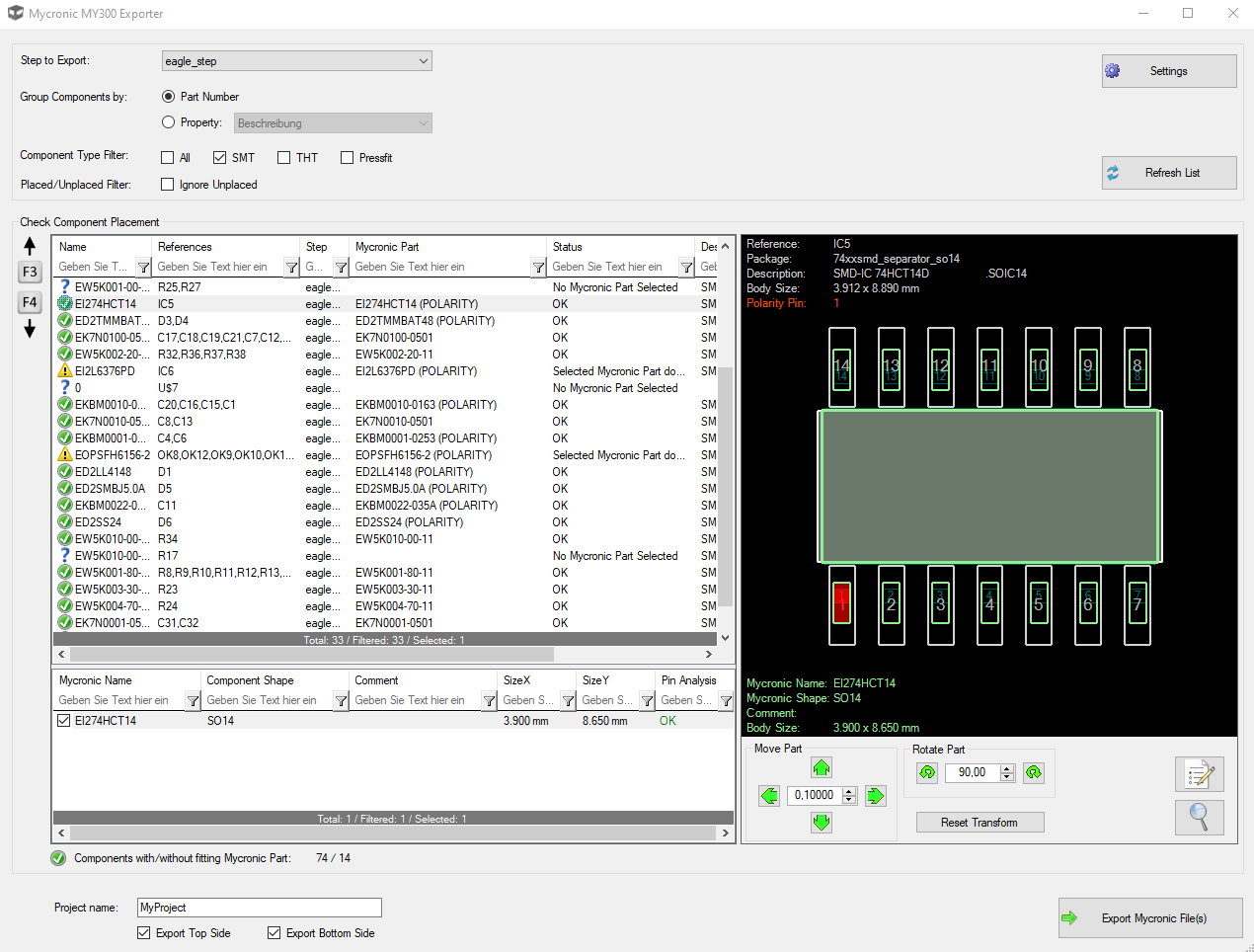
Export Mycronic MY300 format with connection to the machine or with csv library, you have information for pin fitting and polarity pin.
You can filter for technlology like SMT and define export sides and some more:
Export Modus format
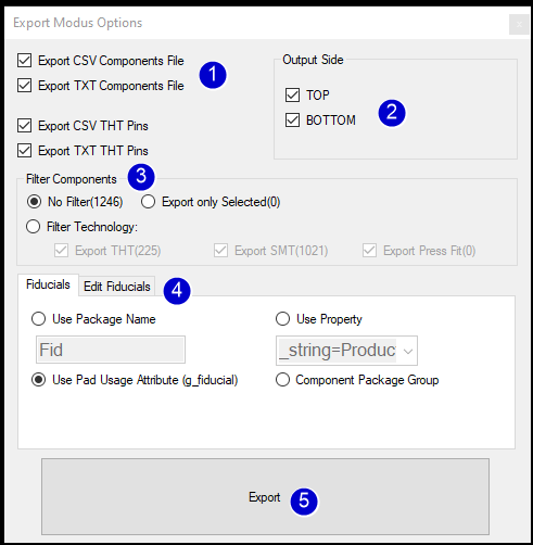
1) Export File selection for components and pins
2) Export Sides (TOP and/or BOTTOM)
3) Filter components e.g. for THT/SMT technology
4) Fiducial definition and overview
5) Export the Modus file(s)
Export TRI Format in one file without specific exta options.
It contains an component list with Position, Rotation, Side, Partname and Packageinfromation.
Export Göpel Standard oder CASCON format

1) Change Output digits or PA Name Attribute (default is package, but in some cases this can be different)
2) Select the output step and the paste layers to export
3) Filter components
4) Define the fiducial markers
5) Change output handling in one or more files and with mirror for bottom side
6) write file(s) for göpel export
This machine export supports the SPI machine aswell as the jtag machine (CASCON).
The files containing information about all relevant components with locations, rotations, package information and details for spi pads with polygon description or standard circle/rectangle definition.
Export and Import Yamaha AOI and PTool format

1) Select Export Type (AOI or P-Tool) and change global settings
2) Define the board and add comments and names
3) Select export layer and side
4) Filter components e.g. technlology SMT
5) Define the fiducials and select output options
6) You can select the Part Name property, in case you want to use internal properties you can just select a other property.
7) Save the Yamaha export
In both formats all important information for components, fiducial markers and meta data for the board available. The P-Tool format is a assembly format to place the components. The AOI format is to check the places components are available in the automatically optical inspection.
Export NDF Format for AOI machines.
The NDF file contains component references with position, Rotation, Placement Side, PartName and Package.
If you want to add new symbols or logos you can handle this symbols in an own library, here is a short video how to add an dmc place holder on the panel edge:
This is only a simple example how to use existing symbol library for and DMC spaceholder Pad. We provide some libraries, but it is also easy to copy existing elements in our managed libraries to store connections directly in PCB-Investigator.
The IDX format is an XML-based messaging system used to exchange design changes between mechanical (MCAD) and electrical (ECAD) design tools, specifically for PCB layouts. It follows the ProSTEP EDMD open schema, which allows incremental updates to be shared between the two types of design systems.
We have added the export for the design and for all production tool frames.
After Importing data in your MCAD Software it can look like this:

Scalable Vector Graphics (SVG) is an XML-based vector image format developed by the W3C for defining two-dimensional graphics. SVG images are scalable without loss of quality, searchable, indexable, and editable with text or vector graphics editors. Supported by all major browsers since 2011, SVG allows for interactivity and animation, and can be embedded directly in HTML documents.
The import has an extra options dialog:

you can switch between converting in full ODB Layer, creating an image layer or handle it as data layer with full zoom but without selection.
With Custom Name option you can switch the layer name to your own text and with unit it is possible to scale the layer.
PCB-Investigator can import Zuken files directly.
Including components, nets and attributes.
PCB-Investigator can import mentor pads files, this direct import allows you to load components, nets and attributes together with all stackup information.
MEK AI is our newest AOI Machine format, this is still in work and only in Beta Version available.
The xml based format containing components with paste information, packages and parts with some properties. The pase pads described as complex features with free polygons or with standard outlines like rounds or rectangles.
The format contains panel information and can handle multible PCBs in family prints.
The Production Tool Editor to define solder frames:

The solder frame definition based on an single PCB with fixing elements as well as down holder with routings for spcial cases like THT components.
The Production Tool Editor to define coating carrier:

The coating carrier base on an standard frame (or special format) with down holder, fixing elements and many more. You can individually change the coating machines to create coating areas and check the frame use legal regions for coating. For better support in the frame you have options to use different routings and depending on the extra material it automatically creates the openings for the coating machine heads.
The Production Tool Editor to define workpiece carrier:

Workpiece carrier containing extra elements and routings, this simple frame create an simple transporting frame with down holders to fix the PCB in the production process.
The Production Tool Editor to define supporting plates:

Supporting plates for pressfit actions in your production line do create routings and documentations for the export files.
The Production Tool Editor to define adapter definitions:

The adapter definition is the most complexe production tool, it contains all standard cases for special testing routines e.g. high voltage checks or vacuum systems. Special handling for connectors, LED Checks, switches or press buttons included.
You can handle stops and fixing elements as well as routings for high components and down holder or supporting stamps. After defining all important elements it is possible to add an example adapter panel to export the adapter package for one DFT Session.
The export contains additional files to create 3D modells like this:
(3D view contains PCB, models for fixing pins, extra electronic and the adapter case)
You can import data from 365 storage directly in the import area.
See more details here
DPF Import has three options:

Flatten Block Content is used for inner block objects to put them directly on the layer
Add Block Dummy Pads create an extra pad with additional block information
Add Text Dummy Pads create dummy pads for text positions with additional information
Connect Library information with your AVL File, with individual importer it can read csv, excel and other files.
Check all components with vidual fitting helper and maybe transform wrong locations or rotations with the simple user interface:

Depending on the MPN and Manufacturer the BOM Expert search for library information and connect them with the open design, this can include properties and step files. You can automatically set no_pop/comp_ignore attributes and use custom actions with an post script to do special actions depending on the imported data.
The Settings containing a list of importers, Searchend Properties and settings to handle not found components. It also has options to add missing entries in an intermediate library and an post script (found by GUID in your favorites).

Unknown => It is not possible to give more details
ReferenceNotInDesign => The reference in imported data is not available in the design
ReferenceNotInAVL => The component in the design has no entry in imported file
NoPartAvailable => The part list do not contain results in the selected library
NoPartSelected => No part selected mean the user has to select one
NotFoundInLib => The library do not contain a fitting item
SelectedPartDoesNotMatch => There is a maybe wrong part selected, please check the selected part
OK => Part is OK
OKUnverified => The pin matiching is not checked but the part is marked as OK
Essemtec export is included in PCB-Investigator V16.1, it connects PCB-Investigator with the Essemtec machine and transfer all important information.
A full description is placed here:
Raster Image Export creates a high resolution image (black and white). It can combine different layers e.g. to cut out the drills and has options for "Anti-Alias", DPI and different performance settings:

Export Koh Young Files for AXI, AOI and SPI with component, package, part and foodprint information
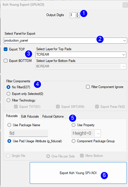
1) Option for output digits
2) Select the output panel
3) Export Top and/or Bottom side with extra layer for the paste definitions
4) Use filters e.g. for THT components or ignore unplaced components
5) Change the fiducial definitions
6) Export the Koh Young KYPcb/xml File(s)
Koh Young CPL Export
Component export for pick and place
