STEP (short for "Standard for the Exchange of Product model data") is a popular exchange format connecting the world of electronics and mechanics. Usually it is used to share 3D models between users with different CAD systems. STEP goes beyond the simple exchange of gemoetry like DXF and IGES. You can integrate all forms of CAD data models (wire, surface and volume models) in the geometry description.
Step Export has two detail areas, first is Standard Export:
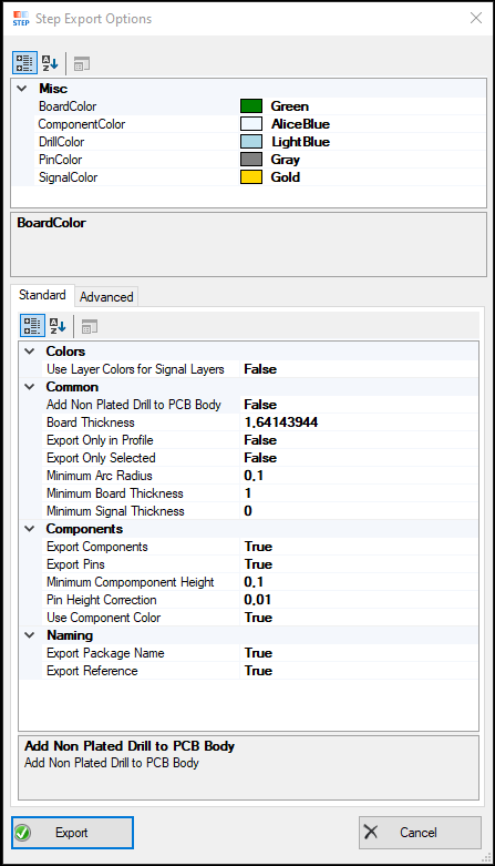
Determines whether the PCB body is exported.
Enables the export of PCB components.
Determines if component pins should be exported.
Defines the color of the PCB board. (Hidden in UI)
Defines the color of components on the PCB. (Hidden in UI)
Defines the color used for signal layers. (Hidden in UI)
Adjusts the height of pins to make them more visible.
Specifies the standard thickness of the board if no stack-up is defined.
Sets a minimum height for components when their height is zero.
Combines objects with the same net in a STEP item.
Exports only the objects within the defined profile.
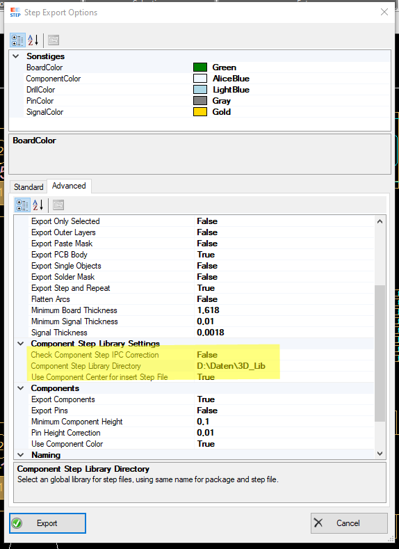
Defines the global library directory for STEP files, ensuring component package names match the STEP file names.
Ensures components follow IPC rotation to match the STEP library if different from package shapes.
Positions all components at the center of CAD bounds by default.
And Second Export Options for Advanced settings:

Export the PCB body.
Export components included in the PCB design.
Export component pins.
Color of the PCB board.
Color used for components.
Color used for signals.
Color used for drill holes.
Color used for pins.
Adjustment for pin height to make them more visible.
Standard board thickness if no stack-up is defined.
Standard layer thickness if no stack-up is defined.
Minimum component height if component height is set to 0.
Minimum board thickness.
Minimum layer thickness for signals.
Minimum arc radius to be exported.
Option to export outer layers of the PCB.
Option to export inner layers of the PCB.
Export only the selected objects.
Use ODB-specified colors for signal layers.
Use the specified component color.
Export reference to the STEP part.
Export package name to the STEP part.
Export net name to the STEP part.
Combine objects with the same net into one STEP item.
Flatten arcs to lines during export.
Export prepregs as layer objects.
Export signal layers in a separate file.
Export component layers in a separate file.
Export signal layers without thickness.
Export drill layers without thickness.
Export drill layer.
Export all visible layers.
Export solder mask layer.
Export paste mask layer.
Export only objects within the profile.
Add non-plated drill holes to the PCB body.
Add routing layers to the PCB body, creating cutouts from panel builder.
Check for sub-steps and export all elements for a complete panel.
The layer that contains the recess elements for the top side of the PCB body.
The layer that contains the recess elements for the bottom side of the PCB body.
Path to the global library for STEP files, using the same name for the package and STEP file.
Activate IPC rotation correction for components if required by the step library.
Insert components at the center of CAD bounds by default.
the new step import converts 3D step files in 2D slices. You can handle complete layers (e.g. with routings or drills), single step files for components (or package definitions), extra electronic and all other step files e.g. housings.
You can use the imported step files for 3D generation (connected to the original step file), it is possible to place the import many times or as replacement for the step export.

In the Step Import dialog you have some options e.g. rotate/scale/translate and auto adjustment (Set Center (0,0)). You see the slice plane in light blue and can also add the CAD data Board outline for exact placing.

(screenshot 3D PCB in adapter with extra electronic and fixing pins)
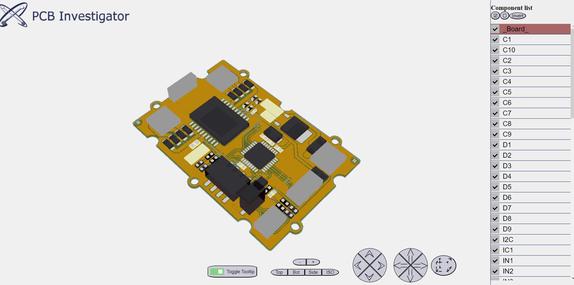
With PCB-Investigator, you have the ability to obtain a realistic 3D view.
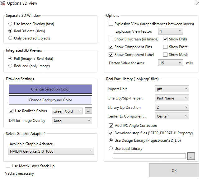
This guide explains how to create accurate 3D views and ensure their inclusion when exporting to various formats such as STEP, OBJ, and WebGL. To do so, follow these steps:
Here, you have three options to choose from:
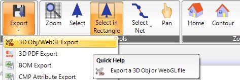
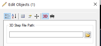
If you wish to export your 3D design, you have the option to do so in STEP, OBJ, STL and WebGL formats.
see more to step format here!

There are some basic settings to match the packages.
Pin Positions are always used, but you can change the Height information of your CAD Data to tolerance value based on the component height or ignore it complete.
Overwrite package and step information defaul by "Ask", this mean there comes a dialog with checkboxes.
How to use the Package Expert firt time?
Here is a short video how to ask Library for all components and set 3D settings: